|
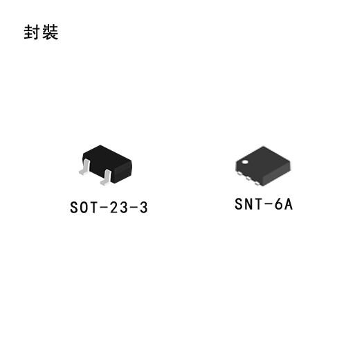
S-1000
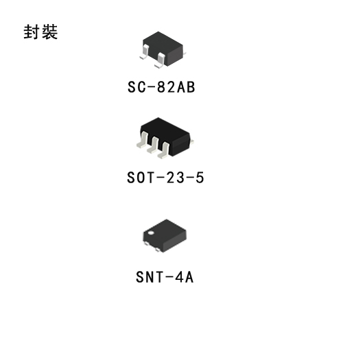
Ultra-Small Package High-Precision Voltage Detector S-1000 Series Description The S-1000 series is a series of high-precision voltage detectors developed using CMOS process. The detection voltage is fixed internally with an accuracy of ��1.0%. It operates with low current consumption of 350 nA typ. Two output forms, Nch open-drain and CMOS output, are available. CMOS voltage detector, S-1000 Series is the most suitable for the portable equipments with ultra low current consumption, high precision and corresponding to the small package.
Features
Applications
|
 S1000Ӣ��.pdf

|
S-808xxC
High-Precision Super-Small Package Voltage Detector S-808xxC Series Description The S-808xxC series is a series of high-precision voltage detectors developed using CMOS process. The detection voltage is fixed internally with an accuracy of ��2.0%. Two output forms, Nch open-drain and CMOS output, are available.
Features
Applications
|

|
S-1009
Super-Low Current Consumption Super High-Accuracy Voltage Detector With Delay Circuit (External Delay Time Setting) S-1009 Series Description The S-1009 Series is a super high-accuracy voltage detectordeveloped using CMOS process. The detection voltage is fixed internally with an accuracy of ��0.5%. It operates with super low current consumption of 270 nA typ.
Features
Applications
|
|
S-809xxC
Super-Small Package High-Precision Voltage Detector with Delay Circuit S-809xxC Series Description The S-809xxC series is a high-precision voltage detector developed using CMOS process. The detection voltage is fixed internally with an accuracy of ��2.0%. A time delayed reset can be accomplished with the addition of an external capacitor. Two output forms, N-channel open-drain and CMOS output, are available.
Features
Applications
|
|
S-801
High-Precision Voltage Detector with Built-in Delay Cricuit S-801 Series Description The S-801 series is a series of high-precision voltage detectors with a built-in delay time generator of fixed time developed using CMOS process. The detection voltage is fixed internally, with an accuracy of ��2.0%. Internal oscillator and counter timer can delay the release signal without external parts. Three delay times 50 ms, 100 ms, and 200 ms are available. Two output forms, Nch open-drain and CMOS output, are available.
Features
Applications
|
|
S-1003
Manual Reset Built-In Delay Circuit (External Delay Time Setting) High-Accuracy Voltage Detector S-1003 Series Description The S-1003 Series is a high-accuracy voltage detector developed using CMOS technology. The detection voltage is fixed internally with an accuracy of ��1.0% (−Vdet �� 2.2 V). It operates with current consumption of 500 nA typ.
Features
Applications
|
|
S-1002
Voltage Detector with SENSE Pin S-1002 Series Description The S-1002 Series is a high-accuracy voltage detector developed using CMOS technology. The detection voltage is fixed internally with an accuracy of ��1.0% (−Vdet(s) �� 2.2 V). It operates with current consumption of 500 nA typ.
Features
Applications
|

|
S-1004
Built-in Delay Circuit (Extenal Delay Time Setting) Voltage Detector with SENSE Pin S-1004 Series Description The S-1004 Series is a high-accuracy voltage detector developed using CMOS technology. The detection voltage is fixed internally with an accuracy of ��1.0% (−Vdet(s) �� 2.2 V). It operates with current consumption of 500 nA typ.
Features
Applications
|
|
S-1011 A/C/J/L
High-Withstand Voltage Built-In Delay Circuit (External Delay Time Setting) Voltage Detector S-1011 Series Description The S-1011 Series is a high-accuracy voltage detector developed using CMOS technology. The detection voltage is fixed internally, and the accuracy of the S-1011 Series A / C / E / G type is ��1.5%. It operates with current consumption of 600 nA typ.
Features
Applications
|

|
S-1011 E/G/N/Q
High-Withstand Voltage Built-In Delay Circuit (External Delay Time Setting) Voltage Detector S-1011 Series Description The S-1011 Series is a high-accuracy voltage detector developed using CMOS technology. The detection voltage is fixed internally, and the accuracy of the S-1011 Series A / C / E / G type is ��1.5%. It operates with current consumption of 600 nA typ.
Features
Application
|
|
S-1410
Low Current Consumption Watchdog Timer with Reset Function S-1410/1411 Description The S-1410/1411 Series is a watchdog timer developed using CMOS technology, which can operate with low current consumption of 3.8 ��A typ. The reset function and the low voltage detection function are available. Features
Application
|

|
S-1411
Low Current Consumption Watchdog Timer with Reset Function S-1410/1411 Description The S-1410/1411 Series is a watchdog timer developed using CMOS technology, which can operate with low current consumption of 3.8 ��A typ. The reset function and the low voltage detection function are available.
Features
Application
|

|
S-1410
Low Current Consumption Watchdog Timer with Reset Function S-1410/1411 Description The S-1410/1411 Series is a watchdog timer developed using CMOS technology, which can operate with low current consumption of 3.8 ��A typ. The reset function and the low voltage detection function are available. Features
Application
|
|
S-1411
Low Current Consumption Watchdog Timer with Reset Function S-1410/1411 Description The S-1410/1411 Series is a watchdog timer developed using CMOS technology, which can operate with low current consumption of 3.8 ��A typ. The reset function and the low voltage detection function are available.
Features
Application
|

|
S-8351
Super-Small Package PFM Control Step-Up Switching Regulator (DC/DC Converter ICs) S-8351/8352 Series Description The S-8351/8352 series is a CMOS PFM-control step-up switching regulator (DC/DC Converter ICs) that mainly consists of a reference voltage source, an oscillator, and a comparator. The PFM controller allows the duty ratio to be automatically switched according to the load (light load: 50%, high output current: 75%), enabling products with a low ripple over a wide range, high efficiency, and high output current (product types A, B, and D). Products with a fixed duty ratio of 75% are also available (product type C). With the S-8351 series, a step-up switching regulator (DC/DC Converter ICs) can be configured by using an external coil, capacitor, and diode. The built-in MOS FET is turned off by a protection circuit when the voltage at the CONT pin exceeds the limit to prevent it from being damaged. This feature, along with the mini package and low current consumption, makes the S-8351 series ideal for applications such as the power supply unit of portable equipment. The S-8352 series, which features an external transistor, is suitable for applications requiring a high output current.
Features
Applications
|
|
S-8352
Super-Small Package PFM Control Step-Up Switching Regulator (DC/DC Converter ICs) S-8351/8352 Series Description The S-8351/8352 series is a CMOS PFM-control step-up switching regulator (DC/DC Converter ICs) that mainly consists of a reference voltage source, an oscillator, and a comparator. The PFM controller allows the duty ratio to be automatically switched according to the load (light load: 50%, high output current: 75%), enabling products with a low ripple over a wide range, high efficiency, and high output current (product types A, B, and D). Products with a fixed duty ratio of 75% are also available (product type C). With the S-8351 series, a step-up switching regulator (DC/DC Converter ICs) can be configured by using an external coil, capacitor, and diode. The built-in MOS FET is turned off by a protection circuit when the voltage at the CONT pin exceeds the limit to prevent it from being damaged. This feature, along with the mini package and low current consumption, makes the S-8351 series ideal for applications such as the power supply unit of portable equipment. The S-8352 series, which features an external transistor, is suitable for applications requiring a high output current.
Features
Applications
|

|
S-8353
Super-Small Package PWM Control, PWM/PFM Control Step-Up Switching Regulator (DC/DC Converter ICs) S-8353/8354 Series Description The S-8353/54 Series is a CMOS step-up switching regulator (DC/DC Converter ICs) which mainly consists of a reference voltage source, an oscillation circuit, a power MOS FET, an error amplifier, a phase compensation circuit, a PWM controller (S-8353) and a PWM/PFM switching controller (S-8354).The step-up switching regulator (DC/DC Converter ICs) can be configured simply by attaching a coil, capacitor, and diode externally. In addition to the above features, the small package and low power consumption of this series make it ideal for portable device applications requiring high efficiency.The S-8353 Series realizes low ripple, high efficiency, and excellent transient characteristics due to its PWM controller, which can vary the duty ratio linearly from 0% to 83% (from 0% to 78% for 250 kHz models), optimally-designed error amplifier, and phase compensation circuits. The S-8354 Series features a PWM/PFM switching controller that can switch the operation to a PFM controller with a duty ratio is 15% under a light load to prevent a decline in the efficiency due to the IC operating current.
Features
Applications
|

|
S-8354
Super-Small Package PWM Control, PWM/PFM Control Step-Up Switching Regulator (DC/DC Converter ICs) S-8353/8354 Series Description The S-8353/54 Series is a CMOS step-up switching regulator (DC/DC Converter ICs) which mainly consists of a reference voltage source, an oscillation circuit, a power MOS FET, an error amplifier, a phase compensation circuit, a PWM controller (S-8353) and a PWM/PFM switching controller (S-8354). The step-up switching regulator (DC/DC Converter ICs) can be configured simply by attaching a coil, capacitor, and diode externally. In addition to the above features, the small package and low power consumption of this series make it ideal for portable device applications requiring high efficiency. The S-8353 Series realizes low ripple, high efficiency, and excellent transient characteristics due to its PWM controller, which can vary the duty ratio linearly from 0% to 83% (from 0% to 78% for 250 kHz models), optimally-designed error amplifier, and phase compensation circuits. The S-8354 Series features a PWM/PFM switching controller that can switch the operation to a PFM controller with a duty ratio is 15% under a light load to prevent a decline in the efficiency due to the IC operating current.
Features
Applications
|
|
S-8363
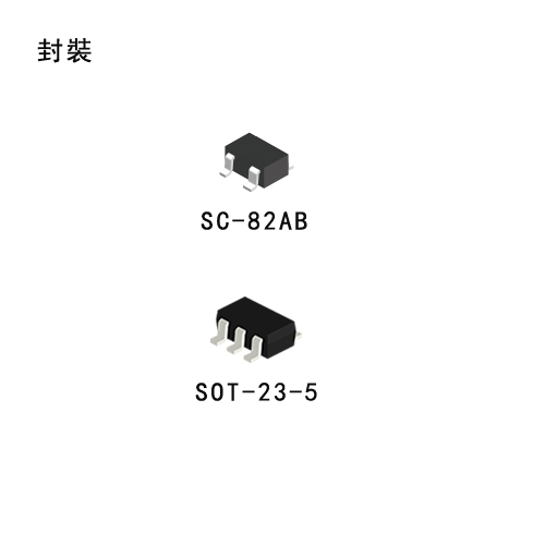
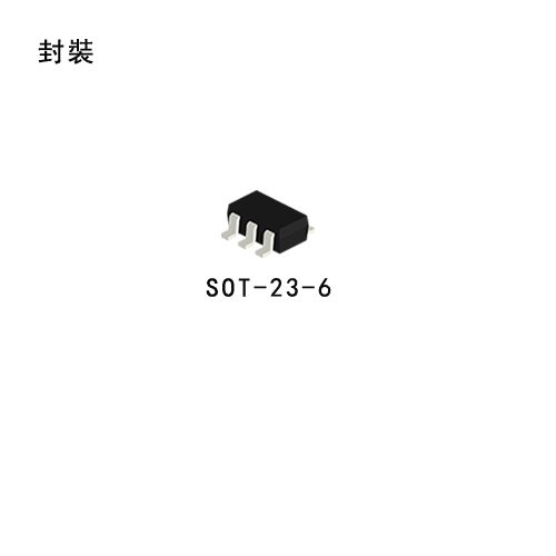
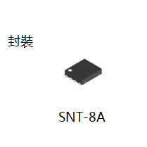
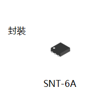
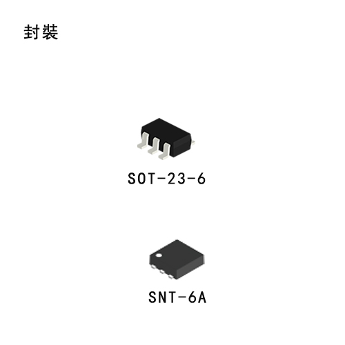
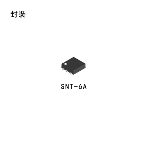
Step-up, Super-small Package, 1.2 MHz PWM / PFM Switchable Switchin Regulator S-8363 Series Description The S-8363 Series is a CMOS step-up switching regulator which consists of a referencevoltage source, an oscillation circuit, an error amplifier, a phase compensation circuit, a current limit circuit, and a start-up circuit. Due to the operation of the PWM / PFM switching control, pulses are skipped under the light load operation and the S-8363 Series prevents decrease in efficiency caused by IC��s operating current. The S-8363 Series is capable of start-up from 0.9 V (Iout = 1 mA) by the start-up circuit, and is suitable for applications which use one dry cell. The output voltage is freely settable from 1.8 V to 5.0 V by external parts. Ceramic capacitors can be used for output capacitor. Small packages SNT-6A and SOT-23-6 enable high-density mounting.
Features
Applications
|

|
S-8355
Super-Small Package PWM Control, PWM/PFM Control Step-Up Switching Regulator (DC/DC Converter ICs) S-8355/56/57/58 Series Description The S-8355/56/57/58 Series is a CMOS step-up switching regulator (DC/DC Converter ICs) which mainly consists of a reference voltage source, an oscillation circuit, an error amplifier, a phase compensation circuit, a PWM control circuit (S-8355/57) and a PWM/PFM switching control circuit (S-8356/58). With an external low-ON-resistance Nch Power MOS, this product is applicable to applications requiring high efficiency and high output current. The S-8355/57 Series realizes low ripple, high efficiency, and excellent transient characteristics with the PWM control circuit whose duty ratio can vary from 0 % to 83 % (from 0 % to 78 % for 250 kHz and 300 kHz models), the best-designed error amplifier and phase compensation circuits. The S-8356/58 Series switches its operation to the PFM control circuit whose duty ratio is 15 % with to the PWM/PFM switching control circuit under a light load and to prevent decline in the efficiency by IC operation current.
Features
Applications
|

|
S-8356
Super-Small Package PWM Control, PWM/PFM Control Step-Up Switching Regulator (DC/DC Converter ICs) S-8355/56/57/58 Series Description The S-8355/56/57/58 Series is a CMOS step-up switching regulator (DC/DC Converter ICs) which mainly consists of a reference voltage source, an oscillation circuit, an error amplifier, a phase compensation circuit, a PWM control circuit (S-8355/57) and a PWM/PFM switching control circuit (S-8356/58). With an external low-ON-resistance Nch Power MOS, this product is applicable to applications requiring high efficiency and high output current. The S-8355/57 Series realizes low ripple, high efficiency, and excellent transient characteristics with the PWM control circuit whose duty ratio can vary from 0 % to 83 % (from 0 % to 78 % for 250 kHz and 300 kHz models), the best-designed error amplifier and phase compensation circuits. The S-8356/58 Series switches its operation to the PFM control circuit whose duty ratio is 15 % with to the PWM/PFM switching control circuit under a light load and to prevent decline in the efficiency by IC operation current.
Features
Applications
|

|
S-8357
Super-Small Package PWM Control, PWM/PFM Control Step-Up Switching Regulator (DC/DC Converter ICs) S-8355/56/57/58 Series Description The S-8355/56/57/58 Series is a CMOS step-up switching regulator (DC/DC Converter ICs) which mainly consists of a reference voltage source, an oscillation circuit, an error amplifier, a phase compensation circuit, a PWM control circuit (S-8355/57) and a PWM/PFM switching control circuit (S-8356/58). With an external low-ON-resistance Nch Power MOS, this product is applicable to applications requiring high efficiency and high output current. The S-8355/57 Series realizes low ripple, high efficiency, and excellent transient characteristics with the PWM control circuit whose duty ratio can vary from 0 % to 83 % (from 0 % to 78 % for 250 kHz and 300 kHz models), the best-designed error amplifier and phase compensation circuits. The S-8356/58 Series switches its operation to the PFM control circuit whose duty ratio is 15 % with to the PWM/PFM switching control circuit under a light load and to prevent decline in the efficiency by IC operation current.
Features
Applications
|

|
S-8358
Super-Small Package PWM Control, PWM/PFM Control Step-Up Switching Regulator (DC/DC Converter ICs) S-8355/56/57/58 Series Description The S-8355/56/57/58 Series is a CMOS step-up switching regulator (DC/DC Converter ICs) which mainly consists of a reference voltage source, an oscillation circuit, an error amplifier, a phase compensation circuit, a PWM control circuit (S-8355/57) and a PWM/PFM switching control circuit (S-8356/58). With an external low-ON-resistance Nch Power MOS, this product is applicable to applications requiring high efficiency and high output current. The S-8355/57 Series realizes low ripple, high efficiency, and excellent transient characteristics with the PWM control circuit whose duty ratio can vary from 0 % to 83 % (from 0 % to 78 % for 250 kHz and 300 kHz models), the best-designed error amplifier and phase compensation circuits. The S-8356/58 Series switches its operation to the PFM control circuit whose duty ratio is 15 % with to the PWM/PFM switching control circuit under a light load and to prevent decline in the efficiency by IC operation current.
Features
Applications
|

|
S-8365
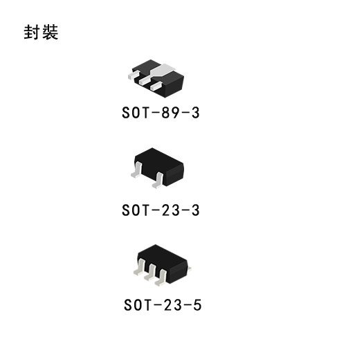
Step-Up, Super-Small Package, 1.2 MHz PWM Control or PWM/PFM Switchable Switching Regulator Controller S-8365/8366 Series Description The S-8365/8366 Series is a CMOS step-up switching regulator controller which mainly consists of a reference voltage source, an oscillation circuit, an error amplifier, a phase compensation circuit, a timer latch short-circuit protection circuit, a PWM control circuit (S-8365 Series) and a PWM / PFM switching control circuit (S-8366 Series). With an external low-ON-resistance Nch Power MOS, this product is ideal for applications requiring high efficiency and a high output current. The S-8365 Series efficiently works on voltage��s condition of large I/O difference due to the PWM control circuit linearly varies the duty ratio to 90%. During light-load, the S-8366 Series switches its operation to the PFM control by the PWM / PFM switching control circuit in order to prevent efficiency decline due to the IC operating current. Ceramic capacitors can be used for output capacitor. Small packages SNT-6A, SOT-23-5 and SOT-23-6 enable high-density mounting.
Features
Applications
|

|
S-8366
Step-Up, Super-Small Package, 1.2 MHz PWM Control or PWM/PFM Switchable Switching Regulator Controller S-8365/8366 Series Description The S-8365/8366 Series is a CMOS step-up switching regulator controller which mainly consists of a reference voltage source, an oscillation circuit, an error amplifier, a phase compensation circuit, a timer latch short-circuit protection circuit, a PWM control circuit (S-8365 Series) and a PWM / PFM switching control circuit (S-8366 Series). With an external low-ON-resistance Nch Power MOS, this product is ideal for applications requiring high efficiency and a high output current. The S-8365 Series efficiently works on voltage��s condition of large I/O difference due to the PWM control circuit linearly varies the duty ratio to 90%. During light-load, the S-8366 Series switches its operation to the PFM control by the PWM / PFM switching control circuit in order to prevent efficiency decline due to the IC operating current. Ceramic capacitors can be used for output capacitor. Small packages SNT-6A, SOT-23-5 and SOT-23-6 enable high-density mounting.
Features
Applications
|

|
S-8340
PWM Control & PWM/PFM Control High Frequency Step-Up Switching Regulator (DC/DC Converter ICs) S-8340/8341 Series Description The S-8340/8341 series consists of CMOS step-up switching regulator (DC/DC Converter ICs)-controllers with PWM control (S-8340) and PWM/PFM switched control (S-8341). These devices contain a reference voltage source, oscillation circuit, error amplifier, phase compensation circuit, PWM control circuit, and other components. Since the oscillation frequency is a high 300 kHz or 600 kHz, with the addition of a small external component, the ICs can function as step-up switching regulators with high efficiency and large output current. The speed of the output stage is enhanced so that the Nch power MOS with a low ON resistance can be switched quickly.
Features
Applications
|

|
S-8341
PWM Control & PWM/PFM Control High Frequency Step-Up Switching Regulator (DC/DC Converter ICs) S-8340/8341 Series Description The S-8340/8341 series consists of CMOS step-up switching regulator (DC/DC Converter ICs)-controllers with PWM control (S-8340) and PWM/PFM switched control (S-8341). These devices contain a reference voltage source, oscillation circuit, error amplifier, phase compensation circuit, PWM control circuit, and other components. Since the oscillation frequency is a high 300 kHz or 600 kHz, with the addition of a small external component, the ICs can function as step-up switching regulators with high efficiency and large output current. The speed of the output stage is enhanced so that the Nch power MOS with a low ON resistance can be switched quickly.
Features
Applications
|
|
S-8333
Step-up, for LCD Bias Supply, 1-channel, PWM Control Switching Regulator Controller S-8333 Series Description The S-8333 Series is a CMOS step-up switching regulator which mainly consists of a reference voltage circuit, an oscillator, an error amplifier, a PWM controller, an under voltage lockout circuit (UVLO), and a timer latch short-circuit protection circuit. Because its minimum operating voltage is as low as 1.8 V, this switching regulator is ideal for the power supply of an LCD or for portable systems that operate on a low voltage. The internal oscillation frequency can be set up to 1.08 MHz, via the resistor connected to the ROSC pin. The maximum duty ratio of PWM control can be controlled by the resistor connected to the RDuty pin. The soft-start function at power application is accomplished by combining the reference voltage control and maximum duty control methods. Even if the voltage of the FB pin is retained lower than the reference voltage due to the factor outside the IC, the output voltage is raised by controlling the maximum duty. The phase compensation and gain value can be adjusted according to the values of the resistor and capacitor connected to the CC pin. Therefore, the operation stability and transient response can be correctly set for each application. The reference voltage accuracy is as high as 1.0 V ��1.5%, and any voltage can be output by using an external output voltage setting resistor. In addition, the delay time of the short-circuit protection circuit can be set by using the capacitor connected to the CSP pin. If the maximum duty condition continues because of short-circuiting, the capacitor externally connected to the CSP pin is charged, and oscillation stops after a specific time. The short-circuit protection function is cancelled when the power supply is raised to the UVLO release voltage after it has been lowered to the UVLO detection voltage. A ceramic capacitor or a tantalum capacitor is used as the output capacitor, depending on the setting. This controller IC allows various settings and selections and employs a small
Features
Applications
|

|
S-8337
Step-up High-frequency, PWM Control Switching Regulator (DC/DC Converter ICs) Controllers S-8337/8338 Series Description The S-8337/38 series is a CMOS step-up switching regulator (DC/DC Converter ICs) which mainly consists of a reference voltage circuit, an oscillator, an error amplifier, a PWM controller, an under voltage lockout circuit (UVLO), and a timer latch short-circuit protection circuit. Because its minimum operating voltage is as low as 1.8 V, this switching regulator (DC/DC Converter ICs) is ideal for the power supply of an LCD or for portable systems that operate on a low voltage. The internal oscillation frequency can be set up to 1.133 MHz, via the resistor connected to the ROSC pin. With the S-8337 series, the maximum duty ratio of PWM control can be controlled by the resistor connected to the RDuty pin. With the S-8338 series, the maximum duty ratio is fixed (to 88%). The phase compensation and gain value can be adjusted according to the values of the resistor and capacitor connected to the CC pin. Therefore, the operation stability and transient response can be correctly set for each application. The reference voltage accuracy is as high as 1.0 V ��1.5%, and any voltage can be output by using an external output voltage setting resistor. In addition, the delay time of the short-circuit protection circuit can be set by using the capacitor connected to the CSP pin. If the maximum duty condition continues because of short-circuiting, the capacitor externally connected to the CSP pin is charged, and oscillation stops after a specific time. This condition is cleared by re-application of power or by setting the switching regulator(DC/DC Converter ICs) (S-8338 series) to the shutdown status. A ceramic capacitor or a tantalum capacitor is used as the output capacitor, depending on the setting. This controller IC allows various settings and selections and employs a small package, making it very easy to use.
Features
Applications
|

|
S-8338
Step-up High-frequency, PWM Control Switching Regulator (DC/DC Converter ICs) Controllers S-8337/8338 Series Description The S-8337/38 series is a CMOS step-up switching regulator (DC/DC Converter ICs) which mainly consists of a reference voltage circuit, an oscillator, an error amplifier, a PWM controller, an under voltage lockout circuit (UVLO), and a timer latch short-circuit protection circuit. Because its minimum operating voltage is as low as 1.8 V, this switching regulator (DC/DC Converter ICs) is ideal for the power supply of an LCD or for portable systems that operate on a low voltage. The internal oscillation frequency can be set up to 1.133 MHz, via the resistor connected to the ROSC pin. With the S-8337 series, the maximum duty ratio of PWM control can be controlled by the resistor connected to the RDuty pin. With the S-8338 series, the maximum duty ratio is fixed (to 88%). The phase compensation and gain value can be adjusted according to the values of the resistor and capacitor connected to the CC pin. Therefore, the operation stability and transient response can be correctly set for each application. The reference voltage accuracy is as high as 1.0 V ��1.5%, and any voltage can be output by using an external output voltage setting resistor. In addition, the delay time of the short-circuit protection circuit can be set by using the capacitor connected to the CSP pin. If the maximum duty condition continues because of short-circuiting, the capacitor externally connected to the CSP pin is charged, and oscillation stops after a specific time. This condition is cleared by re-application of power or by setting the switching regulator(DC/DC Converter ICs) (S-8338 series) to the shutdown status. A ceramic capacitor or a tantalum capacitor is used as the output capacitor, depending on the setting. This controller IC allows various settings and selections and employs a small package, making it very easy to use.
Features
Applications
|
|
S-8550
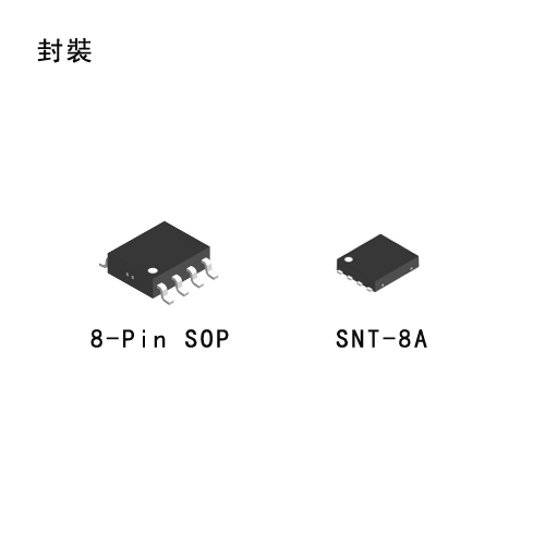
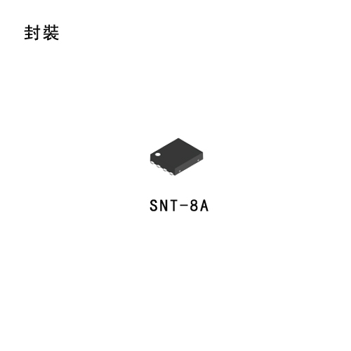
Step-Down, Built-in FET, Synchronous Rectification, PWM Control Switching Regulator (DC/DC Converter ICs) S-8550 Series Description The S-8550 Series is a CMOS synchronous rectification step-down switching regulator which mainly consists of a reference voltage circuit, an oscillator, an error amplifier, a phase compensation circuit, a PWM controller, an under voltage lockout circuit (UVLO), a current limit circuit, and a power MOS FET. The oscillation frequency is high at 1.2 MHz, so a high efficiency, large output current, step-down switching regulator can be achieved by using small external parts. The built-in synchronous rectification circuit makes achieving high efficiency easier compared with conventional step-down switching regulators. A ceramic capacitor can be used as an output capacitor. High-density mounting is supported by adopting packages small SOT-23-5 and super-small and thin SNT-8A.
Features
Applications
|

|
S-8520
PWM Control & PWM/PFM Control Step-Down Switching Regulator (DC/DC Converter ICs) S-8520/8521 Series Description The S-8520/8521 series consists of CMOS step-down switching regulator (DC/DC Converter ICs)-controllers with PWM-control (S-8520) and PWM/PFM-switched control (S-8521). These devices contain a reference voltage source, oscillation circuit, error amplifier, and other components. Features
Applications
|

|
S-8521
PWM Control & PWM/PFM Control Step-Down Switching Regulator (DC/DC Converter ICs) S-8520/8521 Series Description The S-8520/8521 series consists of CMOS step-down switching regulator (DC/DC Converter ICs)-controllers with PWM-control (S-8520) and PWM/PFM-switched control (S-8521). These devices contain a reference voltage source, oscillation circuit, error amplifier, and other components. Features
Applications
|

|
S-8540
PWM Control & PWM/PFM Control High Frequency Step-Down Switching Regulator (DC/DC Converter ICs) S-8540/8541 Series Description The S-8540/8541 series is a family of CMOS step-down switching regulator (DC/DC Converter ICs) controllers with PWM control (S-8540) and PWM/PFM switchover control (S-8541). These devices consist of a reference voltage source, oscillation circuit, an error amplifier, phase compensation circuit, PWM control circuit, current limit circuit. A high efficiency and large current switching regulator (DC/DC Converter ICs) is realized with the help of small external components due to the high oscillation frequency, 300 kHz and 600 kHz. The S-8540 provides low-ripple voltage, high efficiency, and excellent transient characteristics which come form the PMW control circuit capable of varying the duty ratio linearly from 0% to 100%, the optimized error amplifier, and the phase compensation circuit. The S-8541 operates under PWM control when the duty ratio is 29% or higher and operates under PFM control when the duty ratio is less than 29% to ensure high efficiency over all load range. These controllers serve as ideal main power supply units for portable devices due to the high oscillation frequencies together with the small 8-pin MSOP package.
Features
Applications
|

|
S-8541
PWM Control & PWM/PFM Control High Frequency Step-Down Switching Regulator (DC/DC Converter ICs) S-8540/8541 Series Description The S-8540/8541 series is a family of CMOS step-down switching regulator (DC/DC Converter ICs) controllers with PWM control (S-8540) and PWM/PFM switchover control (S-8541). These devices consist of a reference voltage source, oscillation circuit, an error amplifier, phase compensation circuit, PWM control circuit, current limit circuit. A high efficiency and large current switching regulator (DC/DC Converter ICs) is realized with the help of small external components due to the high oscillation frequency, 300 kHz and 600 kHz. The S-8540 provides low-ripple voltage, high efficiency, and excellent transient characteristics which come form the PMW control circuit capable of varying the duty ratio linearly from 0% to 100%, the optimized error amplifier, and the phase compensation circuit. The S-8541 operates under PWM control when the duty ratio is 29% or higher and operates under PFM control when the duty ratio is less than 29% to ensure high efficiency over all load range. These controllers serve as ideal main power supply units for portable devices due to the high oscillation frequencies together with the small 8-pin MSOP package.
Features
Applications
|
|
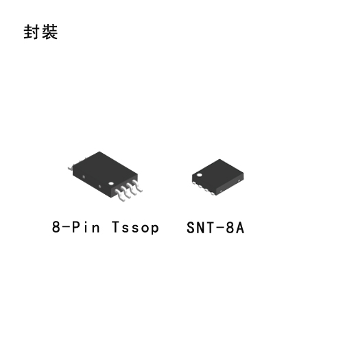
S-8533
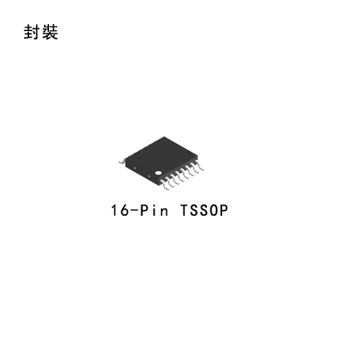
Synchronous PWM Control Step-Down Switching Regulator (DC/DC Converter ICs) S-8533 Series Description The S-8533 series is a synchronous PWM control CMOS step-down switching regulator (DC/DC Converter ICs) controller that includes a reference voltage source, synchronous circuit, an oscillation circuit, an error amplifier, a phase compensation circuit, and a PWM controller. An efficient step-down switching regulator (DC/DC Converter ICs) can be realized simply by adding external Pch and Nch power MOSFETs, one coil, and three capacitors. Since the oscillation frequency is a high 300 kHz, the S-8533 can be used to configure a high efficiency step-down switching regulator (DC/DC Converter ICs) capable of driving high output current using small external components and a 3 to 10% in-crease in efficiency is obtained compared to conventional step-down switching regulators(DC/DC Converter ICs). The 8-Pin TSSOP and high oscillation frequency make the S-8533 ideal as the main power supply for portable devices.
Features
Applications
|
|
S-85S0P
Supply Voltage Divided Output, 5.5 V Input, 50 mA Synchronous Step-down switching Regulator with 260 nA Quiescent Current S-85S0P Series Describe: The S-85S0P Series introduces own distinctive low power consumption control and COT (Constant On-Time) control, features ultra low current consumption (260 nA quiescent current) and fast transient response, operates at PFM control. The S-85S0P Series realizes high efficiency in a wide range of load current consumption and provides strong support forextended period operation of mobile devices and wearable devices which are equipped with compact batteries. Features: DC-DC converter block • Ultra low current consumption: 260 nA quiescent current • Efficiency (when under 100 ��A load): 90.5% • Fast transient response: COT control • Input voltage: 2.2 V to 5.5 V • Output voltage: 0.7 V to 2.5 V, in 0.05 V step 2.6 V to 3.9 V, in 0.1 V step • Output voltage accuracy: ��1.5% (1.0 V �� VOUT �� 3.9 V) ��15 mV (0.7 V �� VOUT < 1.0 V) • High side power MOS FET on-resistance: 420 m�� • Low side power MOS FET on-resistance: 320 m�� • Soft-start function: 1 ms typ. • Under voltage lockout function (UVLO): 1.8 V typ. (detection voltage) • Thermal shutdown function: 135��C typ. (detection temperature) • Overcurrent protection function: 300 mA (at L = 2.2 ��H) • Automatic recovery type short-circuit protection function: Hiccup control • Input and output capacitors: Ceramic capacitor compatible Supply voltage divider block • Low current consumption: 280 nA typ. • Input voltage: 1.5 V to 5.5 V • Output voltage: VIN/2 (S-85S0PCxx) VIN/3 (S-85S0PDxx) Overall • Operation temperature range: Ta = −40��C to +85��C • Lead-free (Sn 100%), halogen-free Applications: • Wearable device • Bluetooth device • Wireless sensor network device • Healthcare equipment • Smart meter • Portable game device |

|
S-85S1P
Supply Voltage Divided Output, 5.5 V Input, 200 mA Synchronous Step-down Switching Regulator with 260 nA Quiescent Current S-85S1P Series Describe: The S-85S1P Series introduces own distinctive low power consumption control and COT (Constant On-Time) control and features ultra low current consumption and fast transient response. PWM / PFM switching control automatically switches to PFM control when under light load, and the IC operates at ultra low current consumption of 260 nA quiescent current. The S-85S1P Series realizes high efficiency in a wide range of load current consumption and provides strong support for extended period operation of mobile devices and wearable devices which are equipped with compact batteries. Features: DC-DC converter block • Ultra low current consumption: 260 nA quiescent current • Efficiency (when under 100 ��A load): 90.5% • Fast transient response: COT control • Input voltage: 2.2 V to 5.5 V • Output voltage: 0.7 V to 2.5 V, in 0.05 V step 2.6 V to 3.9 V, in 0.1 V step • Output voltage accuracy: ��1.5% (1.0 V �� VOUT �� 3.9 V) ��15 mV (0.7 V �� VOUT < 1.0 V) • Switching frequency: 1.0 MHz (at PWM operation) • High side power MOS FET on-resistance: 420 m�� • Low side power MOS FET on-resistance: 320 m�� • Soft-start function: 1 ms typ. • Under voltage lockout function (UVLO): 1.8 V typ. (detection voltage) • Thermal shutdown function: 135��C typ. (detection temperature) • Overcurrent protection function: 450 mA (at L = 2.2 ��H) • Automatic recovery type short-circuit protection function:Hiccup control • Input and output capacitors: Ceramic capacitor compatible Supply voltage divider block • Low current consumption: 280 nA typ. • Input voltage: 1.5 V to 5.5 V • Output voltage: VIN/2 (S-85S1PCxx) VIN/3 (S-85S1PDxx) Overall • Operation temperature range: Ta = −40��C to +85��C • Lead-free (Sn 100%), halogen-free Applications: • Wearable device • Bluetooth device • Wireless sensor network device • Healthcare equipment • Smart meter • Portable game device |

|
S-85S0A
5.5 V Input, 50 mA Synchronous Step-Down Switching Regulator with 260 nA Quiescent Current S-85S0A Series Describe: The S-85S0A Series introduces own distinctive low power consumption control and COT (Constant On-Time) control, features ultra low current consumption (260 nA quiescent current) and fast transient response, operates at PFM control. The S-85S0A Series realizes high efficiency in a wide range of load current consumption and provides strong support for extended period operation of mobile devices and wearable devices which are equipped with compact batteries. Features: • Ultra low current consumption: 260 nA quiescent current • Efficiency (when under 100 ��A load): 90.5% • Fast transient response: COT control • Input voltage: 2.2 V to 5.5 V • Output voltage: 0.7 V to 2.5 V, in 0.05 V stepr 2.6 V to 3.9 V, in 0.1 V step • Output voltage accuracy: ��1.5% (1.0 V �� VOUT �� 3.9 V) ��15 mV (0.7 V �� VOUT < 1.0 V) • High side power MOS FET on-resistance: 420 m�� • Low side power MOS FET on-resistance: 320 m�� • Soft-start function: 1 ms typ. • Under voltage lockout function (UVLO): 1.8 V typ. (detection voltage) • Thermal shutdown function: 135��C typ. (detection temperature) • Overcurrent protection function: 300 mA (at L = 2.2 ��H) • Automatic recovery type short-circuit protection function:Hiccup control • Input and output capacitors: Ceramic capacitor compatible • Operation temperature range: Ta = −40��C to +85��C • Lead-free (Sn 100%), halogen-free Applications: • Wearable device • Bluetooth device • Wireless sensor network device • Healthcare equipment • Smart meter • Portable game device |
|
S-85S1A
5.5v Input, 200mA Synchronous Step-Down Switching Regulator with 260nA Quiescent Current S-85S1A Series Describe: The S-85S1A Series introduces own distinctive low power consumption control and COT (Constant On-Time) control and features ultra low current consumption and fast transient response. PWM / PFM switching control automatically switches to PFM control when under light load, and the IC operates at ultra low current consumption of 260 nA quiescent current. The S-85S1A Series realizes high efficiency in a wide range of load current consumption and provides strong support for extended period operation of mobile devices and wearable devices which are equipped with compact batteries. Features: • Ultra low current consumption: 260 nA quiescent current • Efficiency (when under 100 ��A load): 90.5% • Fast transient response: COT control • Input voltage: 2.2 V to 5.5 V • Output voltage: 0.7 V to 2.5 V, in 0.05 V step 2.6 V to 3.9 V, in 0.1 V step • Output voltage accuracy: ��1.5% (1.0 V �� VOUT �� 3.9 V) ��15 mV (0.7 V �� VOUT < 1.0 V) • Switching frequency: 1.0 MHz (at PWM operation) • High side power MOS FET on-resistance: 420 m�� • Low side power MOS FET on-resistance: 320 m�� • Soft-start function: 1 ms typ. • Under voltage lockout function (UVLO): 1.8 V typ. (detection voltage) • Thermal shutdown function: 135��C typ. (detection temperature) • Overcurrent protection function: 450 mA (at L = 2.2 ��H) • Automatic recovery type short-circuit protection function:Hiccup control • Input and output capacitors: Ceramic capacitor compatible • Operation temperature range: Ta = −40��C to +85��C • Lead-free (Sn 100%), halogen-free Applications: • Wearable device • Bluetooth device • Wireless sensor network device • Healthcare equipment • Smart meter • Portable game device |
|
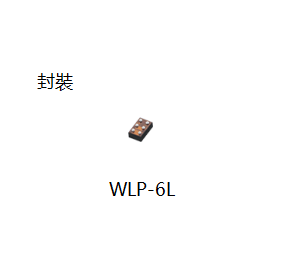
S-85M0A
5.6 V Input, 50 mA, Low EMI, Synchronous Step-down Switching Regulator with 260 nA Quiescent Current S-85M0A Series (WLP product) Describe: The S-85M0A Series introduces own distinctive low power consumption control and COT (Constant On-Time) control, features ultra low current consumption (260 nA quiescent current) and fast transient response, operates at PFM control. The S-85M0A Series realizes high efficiency in a wide range of load current consumption and provides strong support for extended period operation of mobile devices and wearable devices which are equipped with compact batteries. Features: • Ultra low current consumption: 260 nA quiescent current • Efficiency (when under 100 ��A load): 90.5% • Fast transient response: COT control • Input voltage: 2.2 V to 5.6 V • Output voltage: 0.7 V to 2.5 V, in 0.05 V step 2.6 V to 3.9 V, in 0.1 V step • Output voltage accuracy: ��1.5% (1.0 V �� VOUT �� 3.9 V) ��15 mV (0.7 V �� VOUT < 1.0 V) • High side power MOS FET on-resistance: 360 m�� • Low side power MOS FET on-resistance: 250 m�� • Soft-start function: 1 ms typ. • Under voltage lockout function (UVLO): 1.8 V typ. (detection voltage) • Thermal shutdown function: 135��C typ. (detection temperature) • Overcurrent protection function: 300 mA (at L = 2.2 ��H) • Automatic recovery type short-circuit protection function: Hiccup control • Discharge shunt function: Unavailable (S-85M0A Series B type) Available (S-85M0A Series C type) • Input and output capacitors: Ceramic capacitor compatible • Operation temperature range: Ta = −40��C to +85��C • Lead-free, halogen-free Applications: • Wearable device • Bluetooth device • Wireless sensor network device • Healthcare equipment • Smart meter • Portable game device • GPS device |

|
S-85M1A
5.6 V Input, 200 mA, Low EMI, Synchronous Step-down Switching Regulator with 260 nA Quiescent Current S-85M1A Series (WLP product) Describe: The S-85M1A Series introduces own distinctive low power consumption control and COT (Constant On-Time) control and features ultra low current consumption and fast transient response. PWM / PFM switching control automatically switches to PFM control when under light load, and the IC operates at ultra low current consumption of 260 nA quiescent current. The S-85M1A Series realizes high efficiency in a wide range of load current consumption and provides strong support for extended period operation of mobile devices and wearable devices which are equipped with compact batteries. Features: • Ultra low current consumption: 260 nA quiescent current • Efficiency (when under 100 ��A load): 90.5% • Fast transient response: COT control • Input voltage: 2.2 V to 5.6 V • Output voltage: 0.7 V to 2.5 V, in 0.05 V step 2.6 V to 3.9 V, in 0.1 V step • Output voltage accuracy: ��1.5% (1.0 V �� VOUT �� 3.9 V) ��15 mV (0.7 V �� VOUT < 1.0 V) • Switching frequency: 1.0 MHz (at PWM operation) • High side power MOS FET on-resistance: 360 m�� • Low side power MOS FET on-resistance: 250 m�� • Soft-start function: 1 ms typ. • Under voltage lockout function (UVLO): 1.8 V typ. (detection voltage) • Thermal shutdown function: 135��C typ. (detection temperature) • Overcurrent protection function: 450 mA (at L = 2.2 ��H) • Automatic recovery type short-circuit protection function: Hiccup control • Discharge shunt function: Unavailable (S-85M1A Series B type) Available (S-85M1A Series C type) • Input and output capacitors: Ceramic capacitor compatible • Operation temperature range: Ta = −40��C to +85��C • Lead-free, halogen-free Applications: • Wearable device • Bluetooth device • Wireless sensor network device • Healthcare equipment • Smart meter • Portable game device • GPS device |
|
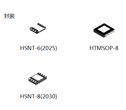
S-8580AC/ S-8580AD/ S-8581AC/ S-8581AD
36V Input, 600 mA Synchronous Step-Down Switching Regulator S-8580AC/ S-8580AD/ S-8581AC/ S-8581AD Series Describe: The S-8580/8581 Series is a step-down switching regulator developed using high withstand voltage CMOS process technologies. This IC has high maximum operation voltage of 36 V and maintains high-accuracy FB pin voltage at ��1.5%. As suitable packages for high-density mounting, such as small-sized HSNT-6(2025), are adopted, this IC contributes to miniaturization of electronic equipment. PWM control (S-8580 Series) or PWM / PFM switching control (S-8581 Series) can be selected as an option. Since the S-8581 Series, which features PWM / PFM switching control, operates with PWM control under heavy load and automatically switches to PFM control under light load, it achieves high-efficiency operation in accordance with the device��s status. Furthermore, our distinctive PWM / PFM switching control technology suppresses the ripple voltage to be generated in VOUT while PFM control is in operation. Since the S-8580/8581 Series has the built-in synchronous circuit, it achieves high efficiency easier compared with conventional step-down switching regulators. In addition, it has the built-in overcurrent protection circuit which protects the IC and coils from excessive load current as well as a thermal shutdown circuit which prevents damage from heat generation. Features: • Input voltage: 4.0 V to 36.0 V • Output voltage (externally set): 2.5 V to 12.0 V for industrial equipment • Output current: 600 mA • FB pin voltage accuracy: ��1.5% for home electric appliance • Efficiency: 95% • Oscillation frequency: 400 kHz typ. • Overcurrent protection function: 1.2 A typ. (pulse-by-pulse method) • Thermal shutdown function: 170��C typ. (detection temperature) • Short-circuit protection function: Hiccup control, Latch control • 100% duty cycle operation: • Soft-start function: 5.8 ms typ. • Under voltage lockout function (UVLO): 3.35 V typ. (detection voltage) • Input and output capacitors: Ceramic capacitor compatible • Operation temperature range: Ta = −40��C to +85��C • Lead-free (Sn 100%), halogen-free Applications: • Constant-voltage power supply for industrial equipment • Constant-voltage power supply for home electric appliance |

|
S-8580AA/S-8580AB/S-8581AA/S-8581AB
36V Input, 600 mA Synchronous Step-Down Switching Regulator S-8580AA/S-8580AB/S-8581AA/S-8581AB Series Describe: The S-8580/8581 Series is a step-down switching regulator developed using high withstand voltage CMOS process technologies. This IC has high maximum operation voltage of 36 V and maintains high-accuracy FB pin voltage at ��1.5%. As suitable packages for high-density mounting, such as small-sized HSNT-6(2025), are adopted, this IC contributes to miniaturization of electronic equipment. PWM control (S-8580 Series) or PWM / PFM switching control (S-8581 Series) can be selected as an option. Since the S-8581 Series, which features PWM / PFM switching control, operates with PWM control under heavy load and automatically switches to PFM control under light load, it achieves high-efficiency operation in accordance with the device��s status. Furthermore, our distinctive PWM / PFM switching control technology suppresses the ripple voltage to be generated in VOUT while PFM control is in operation. Since the S-8580/8581 Series has the built-in synchronous circuit, it achieves high efficiency easier compared with conventional step-down switching regulators. In addition, it has the built-in overcurrent protection circuit which protects the IC and coils from excessive load current as well as a thermal shutdown circuit which prevents damage from heat generation. Features: • Input voltage: 4.0 V to 36.0 V • Output voltage (externally set): 2.5 V to 30.0 V (S-8580 Series) for industrial equipment 2.5 V to 12.0 V (S-8581 Series) • Output current: 600 mA • FB pin voltage accuracy: ��1.5% for home electric appliance • Efficiency: 91% • Oscillation frequency: 2.2 MHz typ. • Overcurrent protection function: 1.2 A typ. (pulse-by-pulse method) • Thermal shutdown function: 170��C typ. (detection temperature) • Short-circuit protection function: Hiccup control, Latch control • 100% duty cycle operation: • Soft-start function: 5.8 ms typ. • Under voltage lockout function (UVLO): 3.35 V typ. (detection voltage) • Input and output capacitors: Ceramic capacitor compatible • Operation temperature range: Ta = −40��C to +85��C • Lead-free (Sn 100%), halogen-free Applications: • Constant-voltage power supply for industrial equipment • Constant-voltage power supply for home electric appliance |
|
S-77100/77101
Power Sequencer S-77100/77101 Series Description The S-77100/77101 Series is a power sequencer.
Features
Application
|
|
S-8821
Voltage Regulation Step-up Charge Pump DC-DC Converter S-8821 Series Description The S-8821 series is a CMOS step-up charge pump DC-DC converter with a voltage regulation function.
Features
Application
|

|
S-8424A
Battery Backup Switching IC S-8424A Series Description The S-8424A Series is a CMOS IC designed for use in the switching circuits of primary and backup power supplies on a single chip. It consists of two voltage regulators, three voltage detectors, a power supply switch and its controller, as well as other functions.
Features
Application
|

|
S-8425
Battery Backup Switching IC S-8425 Series Description The S-8425 Series is a CMOS IC designed for use in the switching circuits of primary and backup power supplies on a single chip. It consists of three voltage regulators, two voltage detectors, a power supply switch and its controller, as well as other functions.
Features
Application
|
|
S-8426A
Battery Backup Switching IC S-8426A Series Description The S-8426A Series is a CMOS IC designed for use in the switching circuits of primary and backup power supplies on a single chip. It consists of two voltage regulators, three voltage detectors, a power supply switch and its controller, as well as other functions. In addition to the switching function between the primary and backup power supply, the S-8426A Series can provide the micro controllers with three types of voltage detection output signals corresponding to the power supply voltage. Moreover adopting a special sequence for switch control enables the effective use of the backup power supply, making this IC ideal for configuring a backup system.
Features
Application
|

|
S-8240A
Battery Protection IC for 1-cell Pack S-8240A Series Description The S-8240A Series is a protection IC for lithium-ion / lithium polymer rechargeable batteries and includes high-accuracy voltage detection circuits and delay circuits. The S-8240A Series is suitable for protecting 1-cell lithium-ion / lithium polymer rechargeable battery packs from overcharge, overdischarge, and overcurrent. Features
Applications
|
|
S-8240B
Battery Protection IC for 1-cell Pack S-8240B Series Description The S-8240B Series is a protection IC for lithium-ion / lithium polymer rechargeable batteries and includes high-accuracy voltage detection circuits and delay circuits. The S-8240B Series is suitable for protecting 1-cell lithium-ion / lithium polymer rechargeable battery packs from overcharge, overdischarge, and overcurrent. Features
Applications
|

|
S-8200A
Battery Protection IC for 1-Cell Pack S-8200A Series Description The S-8200A Series are protection ICs for single-cell lithium-ion / lithium polymer rechargeable batteries and include high-accuracy voltage detectors and delay circuits. These ICs are suitable for protecting single-cell rechargeable lithium-ion / lithium polymer battery packs from overcharge, overdischarge, and overcurrent. Features
Applications
|

|
S-8211C
Battery Protection IC for 1-Cell Pack S-8211C Series Description The S-8211C Series are protection ICs for single-cell lithium-ion / lithium-polymer rechargeable batteries and include highaccuracy voltage detectors and delay circuits. These ICs are suitable for protecting single-cell rechargeable lithium-ion / lithium-polymer battery packs from overcharge, overdischarge, and overcurrent. Features
Applications
|

|
S-8211D
Battery Protection IC for 1-Cell Pack S-8211D Series Description The S-8211D Series are protection ICs for single-cell lithium-ion / lithium-polymer rechargeable batteries and include high-accuracy voltage detectors and delay circuits. These ICs are suitable for protecting single-cell rechargeable lithium-ion / lithium-polymer battery packs from overcharge, overdischarge, and overcurrent. Features
Applications
|

|
S-8261
Battery Protection IC for 1-Cell Pack S-8261 Series Description The S-8261 series are lithium-ion/lithium polymer rechargeable battery protection ICs incorporating high-accuracy voltage detection circuit and delay circuit. The S-8261 series are suitable for protection of single-cell lithium ion/lithium polymer battery packs from overcharge, overdischarge and overcurrent. Features
Applications
|

|
S-82B1A
Battery Protection IC with Charge-discharge Control Function for 1-Cell Pack S-82B1A Series Description The S-82B1A Series is a protection IC for lithium-ion / lithium polymer rechargeable batteries and includes high-accuracy voltage detection circuits and delay circuits. It is suitable for protecting 1-cell lithium-ion / lithium polymer rechargeable battery packs from overcharge, overdischarge, and overcurrent. The S-82B1A Series has an input pin for charge-discharge control signal, allowing for charge-discharge control with an external signal. Features
Applications
|
|
S-8230A/B
Battery Protection IC with Discharge Control Function for 1-Cell Pack S-8230A/B Series Description The S-8230A/B Series is a protection IC for 1-cell lithium-ion / lithium polymer rechargeable batteries and includes high-accuracy voltage detection circuits and delay circuits. The S-8230A/B Series is suitable for protecting 1-cell lithium-ion / lithium polymer rechargeable battery packs from overcharge, overdischarge, overcurrent, and controlling discharge by external signal. Features
Applications
|

|
S-8250A
Battery Protection IC with Discharge Control Function for 1-Cell Pack S-8250A Series Description The S-8250A Series is a protection IC for 1-cell lithium-ion / lithium polymer rechargeable batteries and includes high-accuracy voltage detection circuits and delay circuits. The S-8250A Series is suitable for protecting 1-cell lithium-ion / lithium polymer rechargeable battery packs from overcharge, overdischarge, overcurrent, and controlling discharge by external signal. By adjusting power supply voltage dependency of discharge overcurrent detection voltage in accordance with ON resistance of the charge-discharge control FET, the S-8250A Series realizes high-accuracy discharge overcurrent detection. Features
Applications
|

|
S-8250B
Battery Protection IC with Discharge Control Function for 1-Cell Pack S-8250B Series Description The S-8250B Series is a protection IC for 1-cell lithium-ion / lithium polymer rechargeable batteries and includes high-accuracy voltage detection circuits and delay circuits. The S-8250B Series is suitable for protecting 1-cell lithium-ion / lithium polymer rechargeable battery packs from overcharge, overdischarge and overcurrent. By adjusting power supply voltage dependency of discharge overcurrent detection voltage in accordance with ON resistance of the charge-discharge control FET, the S-8250B Series realizes high-accuracy discharge overcurrent detection. Features
Applications
|
|
S-82A1A
Battery Protection IC for 1-Cell Pack S-82A1A Series Description The S-82A1A Series is a protection IC for lithium-ion / lithium polymer rechargeable batteries and includes high-accuracy voltage detection circuits and delay circuits. It is suitable for protecting 1-cell lithium-ion / lithium polymer rechargeable battery packs from overcharge, overdischarge, and overcurrent. By using an external overcurrent detection resistor, the S-82A1A Series realizes high-accuracy overcurrent protection with less effect from temperature change. Features
Applications
|

|
S-8252
Battery Protection IC for 2-Serial Cell Pack S-8252 Series Description The S-8252 Series are protection ICs for 2-serial-cell lithium-ion / lithium polymer rechargeable batteries and include highaccuracy voltage detectors and delay circuits.These ICs are suitable for protecting 2-serial-cell rechargeable lithium-ion / lithium polymer battery packs from overcharge,overdischarge, and overcurrent. Features
Applications
|
|
S-8262A
Battery Protection IC for 2-Serial Cell Pack S-8262A Series Description The S-8262A Series is a protection IC for 2-serial-cell lithium-ion / lithium polymer rechargeable batteries and includes high-accuracy voltage detectors and delay circuits. The S-8262A Series has an alarm signal output pin (AO pin) which outputs the alarm detection signal. The alarm detection signal is output prior to the charge control FET signal by overcharge detection. Features
Applications
|

|
S-8253C/D
Battery Protection IC for 2-Serial or 3-Serial Cell Pack S-8253C/D Series Description The S-8253C/D Series is a protection ICs for 2-series or 3-series cell lithium-ion rechargeable battery and includes high-accuracy voltage detector and delay circuit. This IC is suitable for protecting lithium-ion battery packs from overcharge, overdischarge and overcurrent. Features
Applications
|

|
S-8243A/B
Battery Protection IC for 3-Cell Serial Pack S-8243A Series Description The S-8243A/B is a series of lithium-ion rechargeable battery protection ICs incorporating high-accuracy battery protection circuits, a battery monitor amp and a voltage regulator. The S-8243A/B is suitable for protection of 3-serial or 4- serial cell lithium-ion battery packs from overcharge, overdischarge and overcurrent. Features
Applications
|

|
S-8254A
Battery Protection IC for 3-Serial or 4-Serial-Cell Pack S-8254A Series Description The S-8254A series is a protection IC for 3-serial or 4-serial cell lithium ion rechargeable batteries and includes a high-accuracy voltage detector and delay circuit. The S-8254 series protects both 3-serial or 4-serial cells using the SEL pin for switching. Features
Applications
|

|
S-8204A
Battery Protection IC for 3-Serial or 4-Serial-Cell Pack S-8204A Series Description The S-8204A Series includes high-accuracy voltage detection circuits and delay circuits, in single use, makes it possible for users to monitor the status of 3-series or 4-series cell lithium-ion rechargeable battery. By switching the voltage level which is applied to the SEL pin, users are able to use the S-8204A Series either for 3-series or 4-series cell pack. By cascade connection using the S-8204A Series, it is also possible to protect 6-series or more cells(*1) lithium-ion rechargeable battery pack. Features
Applications
|

|
S-8204B
Battery Protection IC for 3-Serial or 4-Serial-Cell Pack S-8204B Series Description The S-8204B Series includes high-accuracy voltage detection circuits and delay circuits, in single use, makes it possible for users to monitor the status of 3-series or 4-series cell lithium-ion rechargeable battery. By switching the voltage level which is applied to the SEL pin, users are able to use the S-8204B Series either for 3-series or 4-series cell pack. By cascade connection using the S-8204B Series, it is also possible to protect 6-series or more cells lithium-ion rechargeable battery pack. Features
Applications
|

|
S-8225A
Battery Monitoring IC for 3-Serial to 5-Serial Cell Pack S-8225A Series Description The S-8225A Series includes a voltage detection circuit with high accuracy and a delay circuit, and can monitor the status of 3-serial to 5-serial cell lithium-ion rechargeable battery in single use. By switching the voltage level which is applied to the SEL1 pin and SEL2 pin, users are able to use the S-8225A Series for 3-serial to 5-serial cell pack. By cascade connection using the S-8225A Series, it is also possible to protect 6-serial or more cells rechargeable lithium-ion battery pack. Features
Applications
|

|
S-8225B
Battery Monitoring IC for 3-Serial to 5-Serial Cell Pack S-8225B Series Description The S-8225B Series includes a voltage detection circuit with high accuracy and a delay circuit, and can monitor the status of 3-serial to 5-serial cell lithium-ion rechargeable battery in single use. By switching the voltage level which is applied to the SEL1 pin and SEL2 pin, users are able to use the S-8225B Series for 3-serial to 5-serial cell pack. Features
Applications
|

|
S-8205A/B
Battery Protection IC for 4-Series or 5-Series Cell Pack S-8205A/B Series Description The S-8205A/B Series includes a voltage detection circuit with high accuracy and a delay circuit, in single use, makes it possible for users to monitor the status of 4-series or 5-series cell lithium-ion rechargeable battery. These ICs are suitable for protecting rechargeable lithium-ion battery packs from overcharge, overdischarge, and overcurrent. Features
Applications
|
|
S-8206A
Battery Protection IC for 1-cell Pack (Secondary Protection) S-8206A Series Description The S-8206A Series is used for secondary protection of lithium-ion / lithium polymer rechargeable batteries, and incorporates a high-accuracy voltage detection circuit and a delay circuit. Features
Applications
|
|
S-8244
Battery Protection IC for 1 to 4 Cells (Secondary Protection) S-8244 Series Description The S-8244 series is used for secondary protection of lithium-ion batteries with from one to four cells, and incorporates a high-precision voltage detector circuit and a delay circuit. Short-circuits between cells accommodate series connection of one to four cells. Features
Applications
|

|
S-8213
Battery Protection IC for 2-Serial / 3-Serial Cell Pack (Secondary Protection) S-8213 Series Description The S-8213 Series is used for secondary protection of lithium-ion rechargeable batteries, and incorporates a high-accuracy voltage detection circuit and a delay circuit. Short-circuits between VC3 to VSS accommodate serial connection of two cells or three cells. Features
Applications
|

|
S-8264A/B/C
Battery Protection IC for 2-Serial to 4-Serial-cell Pack (Secondary Protection) S-8264A/B/C Series Description The S-8264A/B/C Series is used for secondary protection of lithium-ion rechargeable batteries, and incorporates a high-accuracy voltage detection circuit and a delay circuit. Short-circuits between cells accommodate series connection of two to four cells. Features
Applications
|
|
S-8215A
Battery Protection IC for 3-Serial to 5-Serial Cell Pack (Secondary Protection) S-8215A Series Description The S-8215A Series is used for secondary protection of lithium-ion rechargeable batteries, and incorporates high-accuracy voltage detection circuits and delay circuits. Short-circuiting between cells makes it possible for serial connection of 3 cells to 5 cells. Features
Applications
|

|
S-8259A
Battery Monitoring IC for 1-cell Pack S-8259A Series Description The S-8259A Series is an IC including high-accuracy voltage detection circuits and delay circuits. The S-8259A Series is suitable for monitoring overcharge and overdischarge for 1-cell lithium-ion / lithium polymer rechargeable battery packs. Features
Applications
|
|
S-8211E
Battery Protection IC for 1-Cell Pack S-8211E Series Description The S-8211E Series has the high-accuracy voltage detection circuit and the delay circuit. This IC is suitable for monitoring overcharge and overdischarge of 1-cell lithium ion / lithium polymer secondary battery pack. Features
Applications
|

|
S-8209A
Battery Protection IC with Cell-Balance Function S-8209A Series Description The S-8209A Series is a protection IC for lithium-ion / lithium polymer rechargeable batteries and includes a high-accuracy voltage detection circuit and a delay circuit. This IC has a transmission function and two types of cell-balance function so that users are also able to configure a protection circuit with series multi-cell. Features
Applications
|

|
S-8209B
Battery Protection IC with Cell-Balance Function S-8209B Series Description The S-8209B Series is a protection IC for lithium-ion / lithium polymer rechargeable batteries and includes a high-accuracy voltage detection circuit and a delay circuit. This IC has a transmission function and two types of cell-balance function so that users are also able to configure a protection circuit with series multi-cell. Features
Applications
|

|
S-8229
Battery Monitoring IC S-8229 Series Description The S-8229 Series is a battery monitoring IC developed using CMOS technology. Compared with conventional CMOS voltage detectors, the S-8229 Series is ideal for the applications that require high-withstand voltage due to its maximum operation voltage as high as 24 V. The S-8229 Series is capable of confirming the voltage in stages since it detects three voltage values. Features
Applications
|

|
S-8239A
Overcurrent Monitoring IC For Multi-Serial-Cell Pack S-8239A Series Description The S-8239A Series is an overcurrent monitoring IC for multi-serial-cell pack including high-accuracy voltage detection circuits and delay circuits. The S-8239A Series is suitable for protection of lithium-ion / lithium polymer rechargeable battery packs from overcurrent. Features
Applications
|

|
S-8239B
Overcurrent Monitoring IC For Multi-Serial-Cell Pack S-8239B Series Description The S-8239B Series is an overcurrent monitoring IC for multi-serial-cell pack including high-accuracy voltage detection circuits and delay circuits. The S-8239B Series is suitable for protection of lithium-ion / lithium polymer rechargeable battery packs from overcurr Features
Applications
|

|
S-8249
Voltage Monitoring IC with Cell Balancing Function S-8249 Series Description The S-8249 Series is a voltage monitoring IC with a cell balancing function and includes a high-accuracy voltage detection circuit and a delay circuit. The S-8249 Series is suitable for cell balancing and overcharge protection of batteries and capacitors. Features
Applications
|

|
S-82U1A
Battery Protection IC with Alarm Function for 1-Cell Pack S-82U1A Series Describe�� This IC is a protection IC for lithium-ion / lithium polymer rechargeable batteries, which includes high-accuracy voltage detection circuits and delay circuits. It is suitable for protecting 1-cell lithium-ion / lithium polymer rechargeable battery packs from overcharge, overdischarge, and overcurrent. By using an external overcurrent detection resistor, This IC realizes high-accuracy overcurrent protection with less effect from temperature change. The alarm function enables the voltage detection immediately before the overcharge detection. Features��
Overcharge detection voltage 3.500 V to 4.800 V (5 mV step) Accuracy ��12 mV Overcharge release voltage 3.100 V to 4.800 V*1 Accuracy ��50 mV Alarm detection voltage 3.500 V to 4.800 V (5 mV step) Accuracy ��12 mV Alarm hysteresis voltage 0 V, 0.010 V, 0.020 V Accuracy ��5 mV Overdischarge detection voltage 2.000 V to 3.000 V (10 mV step) Accuracy ��50 mV Overdischarge release voltage 2.000 V to 3.400 V*2 Accuracy ��75 mV Discharge overcurrent 1 detection voltage 3 mV to 100 mV (0.5 mV step) Accuracy ��1 mV Discharge overcurrent 2 detection voltage 10 mV to 100 mV (1 mV step) Accuracy ��2 mV Load short-circuiting detection voltage 20 mV to 100 mV (1 mV step) Accuracy ��4.5 mV Charge overcurrent detection voltage −100 mV to −3 mV (0.5 mV step) Accuracy ��1 mV
Release condition of discharge overcurrent status: Load disconnection Release voltage of discharge overcurrent status: Discharge overcurrent release voltage (VRIOV) = VDD �� 0.8 (typ.)
AO pin output logic: Active "H", active "L" AO pin output form: CMOS output, Nch open-drain output Connection when AO pin = "L": VSS pin, VM pin Charge control function: Available, unavailable
During operation: 2.5 ��A typ., 5.0 ��A max. (Ta = +25��C) During power-down: 50 nA max. (Ta = +25��C) During overdischarge: 0.5 ��A max. (Ta = +25��C)
Applications��
|
|
S-82L1A
Battery Protection IC with Alarm Function for 1-Cell Pack S-82L1A Series Describe: The S-82L1A Series is a protection IC for lithium-ion / lithium polymer rechargeable batteries, which includes high-accuracy voltage detection circuits and delay circuits. It is suitable for protecting 1-cell lithium-ion / lithium polymer rechargeable battery packs from overcharge, overdischarge, and overcurrent. The alarm function enables the voltage detection immediately before the overcharge detection. Features:
Overcharge detection voltage 4.200 V to 4.600 V (5 mV step) Accuracy ��12 mV Overcharge release voltage 4.000 V to 4.600 V*1 Accuracy ��50 mV Overdischarge detection voltage 2.000 V to 3.000 V (10 mV step) Accuracy ��50 mV Overdischarge release voltage 2.000 V to 3.400 V*2 Accuracy ��100 mV Alarm status detection voltage 4.200 V to 4.600 V (5 mV step) Accuracy ��12 mV Discharge overcurrent detection voltage 0.003 V to 0.100 V (1 mV step) Accuracy ��3 mV Load short-circuiting detection voltage 0.010 V to 0.100 V (5 mV step) Accuracy ��7 mV Charge overcurrent detection voltage −0.100 V to −0.003 V (1 mV step) Accuracy ��3 mV
Release condition of discharge overcurrent status: Load disconnection Release voltage of discharge overcurrent status: VRIOV = VDD �� 0.8 (typ.)
AO pin output logic: Active "L" AO pin output form: CMOS output, Nch open-drain output Connection when AO pin = "L": VSS pin, VM pin
During operation: 800 nA typ., 1500 nA max. (Ta = +25��C) During power-down: 50 nA max. (Ta = +25��C) During overdischarge: 500 nA max. (Ta = +25��C)
Applications:
|

|
S-82T1A
Battery Protection IC with Alarm Function for 1-Cell Pack S-82T1A Series Describe: This IC is a protection IC for lithium-ion / lithium polymer rechargeable batteries, which includes high-accuracy voltage detection circuits and delay circuits. It is suitable for protecting 1-cell lithium-ion / lithium polymer rechargeable battery packs from overcharge, overdischarge, and overcurrent. By using an external overcurrent detection resistor, This IC realizes high-accuracy overcurrent protection with less effect from temperature change. The alarm function enables the voltage detection immediately before the overcharge detection.
Features:
Overcharge detection voltage 3.500 V to 4.800 V (5 mV step) Accuracy ��12 mV Overcharge release voltage 3.100 V to 4.800 V*1 Accuracy ��50 mV Alarm detection voltage 3.500 V to 4.800 V (5 mV step) Accuracy ��12 mV Alarm hysteresis voltage 0 V, 0.010 V, 0.020 V Accuracy ��5 mV Overdischarge detection voltage 2.000 V to 3.000 V (10 mV step) Accuracy ��50 mV Overdischarge release voltage 2.000 V to 3.400 V*2 Accuracy ��75 mV Discharge overcurrent 1 detection voltage 3 mV to 100 mV (0.5 mV step) Accuracy ��1.5 mV Discharge overcurrent 2 detection voltage 10 mV to 100 mV (1 mV step) Accuracy ��3 mV Load short-circuiting detection voltage 20 mV to 100 mV (1 mV step) Accuracy ��5 mV Charge overcurrent detection voltage −100 mV to −3 mV (0.5 mV step) Accuracy ��1.5 mV
Release condition of discharge overcurrent status: Load disconnection Release voltage of discharge overcurrent status: Discharge overcurrent release voltage (VRIOV) = VDD �� 0.8 (typ.)
AO pin output logic: Active "H", active "L" AO pin output form: CMOS output, Nch open-drain output Connection when AO pin = "L": VSS pin, VM pin Charge control function: Available, unavailable
During operation: 2.5 ��A typ., 5.0 ��A max. (Ta = +25��C) During power-down: 50 nA max. (Ta = +25��C) During overdischarge: 0.5 ��A max. (Ta = +25��C)
Applications:
|
|
S-82V1A
Battery Protection IC with Alarm Function for 1-Cell Pack S-82V1A Series Describe: This IC is a protection IC for lithium-ion / lithium polymer rechargeable batteries, which includes high-accuracy voltage detection circuits and delay circuits. It is suitable for protecting 1-cell lithium-ion / lithium polymer rechargeable battery packs from overcharge, overdischarge, and overcurrent. By using an external overcurrent detection resistor, This IC realizes high-accuracy overcurrent protection with less effect from temperature change. The alarm function enables the voltage detection immediately before the overcharge detection. Features:
Overcharge detection voltage 3.500 V to 4.800 V (5 mV step) Accuracy ��12 mV Overcharge release voltage 3.100 V to 4.800 V*1 Accuracy ��50 mV Alarm detection voltage 3.500 V to 4.800 V (5 mV step) Accuracy ��12 mV Alarm hysteresis voltage 0 V, 0.010 V, 0.020 V Accuracy ��5 mV Overdischarge detection voltage 2.000 V to 3.000 V (10 mV step) Accuracy ��50 mV Overdischarge release voltage 2.000 V to 3.400 V*2 Accuracy ��75 mV Discharge overcurrent 1 detection voltage 3 mV to 100 mV (0.25 mV step) Accuracy ��0.75 mV Discharge overcurrent 2 detection voltage 6 mV to 100 mV (0.5 mV step) Accuracy ��1.5 mV Load short-circuiting detection voltage 20 mV to 100 mV (1 mV step) Accuracy ��4 mV Charge overcurrent detection voltage −100 mV to −3 mV (0.25 mV step) Accuracy ��0.75 mV
Release condition of discharge overcurrent status: Load disconnection Release voltage of discharge overcurrent status: Discharge overcurrent release voltage (VRIOV) = VDD �� 0.8 (typ.)
AO pin output logic: Active "H", active "L" AO pin output form: CMOS output, Nch open-drain output Connection when AO pin = "L": VSS pin, VM pin Charge control function: Available, unavailable
During operation: 2.5 ��A typ., 5.0 ��A max. (Ta = +25��C) During power-down: 50 nA max. (Ta = +25��C) During overdischarge: 0.5 ��A max. (Ta = +25��C)
Applications: Lithium-ion rechargeable battery pack Lithium polymer rechargeable battery pack |
|
S-82C4A/5A
Battery Protection IC for 4-serial to 5-serial Cell Pack S-82C4A/5A Series Describe: This IC is a protection IC for lithium-ion rechargeable batteries, which includes temperature protection circuits, high-accuracy voltage detection circuits, and delay circuits. Temperature protection is possible by connecting an NTC thermistor to the dedicated connection pin. It is suitable for protecting 4-serial or 5-serial cell lithium-ion rechargeable battery packs from overcharge, overdischarge, and overcurrent. Features:
Overcharge detection voltage n 3.900 V to 4.500 V (25 mV step) Accuracy ��20 mV Overcharge release voltage n 3.500 V to 4.500 V*1 Accuracy ��50 mV Overdischarge detection voltage n 2.000 V to 3.200 V (100 mV step) Accuracy ��50 mV Overdischarge release voltage n 2.000 V to 3.400 V*2 Accuracy ��100 mV
Discharge overcurrent 1 detection voltage 10 mV to 200 mV (5 mV step) Accuracy ��5 mV Discharge overcurrent 2 detection voltage 20 mV to 300 mV (5 mV step) Accuracy ��10 mV Load short-circuiting detection voltage 50 mV to 400 mV (10 mV step) Accuracy ��20 mV
Charge overcurrent detection voltage −200 mV to −10 mV (5 mV step) Accuracy ��5 mV
High temperature charge-discharge inhibition temperature +40��C to +85��C (1��C step) Accuracy ��3��C*3 High temperature charge inhibition temperature +40��C to +85��C (1��C step) Accuracy ��3��C*3 Low temperature charge inhibition temperature −40��C to +10��C (1��C step) Accuracy ��3��C*3 Low temperature charge-discharge inhibition temperature −40��C to +10��C (1��C step) Accuracy ��3��C*3
During operation: 5.0 ��A typ., 10 ��A max. (Ta = +25��C) During power-down: 0.1 ��A max. (Ta = +25��C) During power-saving: 0.1 ��A max. (Ta = +25��C)
Applications:
|

|
S-82B1B
Battery Protection IC with Power-saving Function for 1-Cell Pack S-82B1B Series Describe: The S-82B1B Series is a protection IC for lithium-ion / lithium polymer rechargeable batteries and includes high-accuracy voltage detection circuits and delay circuits. It is suitable for protecting 1-cell lithium-ion / lithium polymer rechargeable battery packs from overcharge, overdischarge, and overcurrent. Features: • High-accuracy voltage detection circuit Overcharge detection voltage 3.500 V to 4.600 V (5 mV step) Accuracy +20 mV Overcharge release voltage 3.100 V to 4.600 V*1 Accuracy +50 mV Overdischarge detection voltage 2.000 V to 3.000 V (10 mV step) Accuracy +50 mV Overdischarge release voltage 2.000 V to 3.400 V*2 Accuracy +100 mV Discharge overcurrent detection voltage 1 0.010 V to 0.100 V (1 mV step) Accuracy +3 mV Discharge overcurrent detection voltage 2 0.030 V to 0.200 V (1 mV step) Accuracy +5 mV Load short-circuiting detection voltage 0.050 V to 0.500 V (5 mV step) Accuracy +20 mV Charge overcurrent detection voltage -0.100 V to -0.010 V (1 mV step) Accuracy +3 mV • Detection delay times are generated only by an internal circuit (external capacitors are unnecessary). • Power-saving function PS pin control logic is selectable: Active "H", active "L" PS pin internal resistance connection is selectable: Pull-up, pull-down PS pin internal resistance value is selectable: 1.0 M��, 2.0 M��, 3.0 M��, 4.0 M��, 5.0 M�� • 0 V battery charge function is selectable: Available, unavailable • Power-down function • Release condition of discharge overcurrent status is selectable: Load disconnection, charger connection • Release voltage of discharge overcurrent status is selectable: Discharge overcurrent detection voltage 1 (VDIOV1), Discharge overcurrent release voltage (VRIOV) = VDD��0.8 (typ.) • High-withstand voltage: VM pin and CO pin: Absolute maximum rating 28 V • Wide operation temperature range: Ta = -40��C to +85��C • Low current consumption During operation: 2.0 ��A typ., 4.0 ��A max. (Ta = +25��C) During power-down: 50 nA max. (Ta = +25��C) During power-saving: 50 nA max. (Ta = +25��C) • Lead-free (Sn 100%), halogen-free *1. Overcharge release voltage = Overcharge detection voltage - Overcharge hysteresis voltage (Overcharge hysteresis voltage can be selected as 0 V or from a range of 0.1 V to 0.4 V in 50 mV step.) *2. Overdischarge release voltage = Overdischarge detection voltage + Overdischarge hysteresis voltage (Overdischarge hysteresis voltage can be selected as 0 V or from a range of 0.1 V to 0.7 V in 100 mV step.) Applications: • Lithium-ion rechargeable battery pack • Lithium polymer rechargeable battery pack |
|
S-82A2A/S-82A2B/S-82A2C
Battery Protection IC for 2-Serial-Cell Pack S-82A2A/B/C Series Describe: This IC is a protection IC for lithium-ion / lithium polymer rechargeable batteries, which includes high-accuracy voltage detection circuits and delay circuits. It is suitable for protecting 2-serial-cell lithium-ion / lithium polymer rechargeable battery packs from overcharge, overdischarge, and overcurrent. Use of an external overcurrent detection resistor enables this IC to provide high-accuracy overcurrent protection with less impact from temperature changes. The S-82A2A/C Series has an input pin for charge-discharge control signal (CTL pin), allowing for charge-discharge control with an external signal. The S-82A2B Series has an input pin for power-saving signal (PS pin), allowing for reduction of current consumption by using an external signal to start the power-saving function. Features: • High-accuracy voltage detection circuit Overcharge detection voltage n 3.500 V to 4.800 V (5 mV step) Accuracy ��15 mV Overcharge release voltage n 3.100 V to 4.800 V*1 Accuracy ��50 mV Overdischarge detection voltage n 2.000 V to 3.000 V (10 mV step) Accuracy ��50 mV Overdischarge release voltage n 2.000 V to 3.400 V*2 Accuracy ��75 mV Discharge overcurrent 1 detection voltage 3 mV to 100 mV (0.5 mV step) Accuracy ��1.0 mV Discharge overcurrent 2 detection voltage 10 mV to 100 mV (1 mV step) Accuracy ��3 mV Load short-circuiting detection voltage 20 mV to 100 mV (1 mV step) Accuracy ��5 mV Charge overcurrent detection voltage −100 mV to −3 mV (0.5 mV step) Accuracy ��1.0 mV • Detection delay times are generated only by an internal circuit (external capacitors are unnecessary). • Charge-discharge control function (S-82A2A/C Series) CTL pin control logic: Active "H", active "L" CTL pin internal resistance connection: Pull-up, pull-down CTL pin internal resistance value: 1 M�� to 10 M�� (1 M�� step) • Power-saving function (S-82A2B Series) PS pin control logic: Active "H", active "L" PS pin internal resistance value: 1 M�� to 10 M�� (1 M�� step) • 0 V battery charge: Enabled, inhibited • Power-down function: S-82A2A/C Series: Available, unavailable S-82A2B Series: Available • High-withstand voltage: VM pin and CO pin: Absolute maximum rating 28 V • Wide operation temperature range: Ta = −40��C to +85��C • Low current consumption During operation: 3.0 ��A typ., 6.0 ��A max. (Ta = +25��C) During power-down: 50 nA max. (Ta = +25��C) During overdischarge: 1.0 ��A max. (Ta = +25��C) During power-saving (S-82A2B Series): 50 nA max. (Ta = +25��C) • Lead-free (Sn 100%), halogen-free *1. Overcharge release voltage = Overcharge detection voltage − Overcharge hysteresis voltage (Overcharge hysteresis voltage can be selected as 0 V or from a range of 0.1 V to 0.4 V in 50 mV step.) *2. Overdischarge release voltage = Overdischarge detection voltage + Overdischarge hysteresis voltage (Overdischarge hysteresis voltage can be selected as 0 V or from a range of 0.1 V to 0.7 V in 100 mV step.) Remark n = 1, 2 Applications: • Lithium-ion rechargeable battery pack • Lithium polymer rechargeable battery pack |
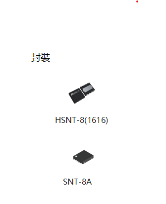
|
S-82C2B/C
Battery Protection IC for 2-serial-cell PacK S-82C2B/C Series Describes: This IC is a protection IC for lithium-ion / lithium polymer rechargeable batteries, which includes high-accuracy voltage detection circuits and delay circuits. It is suitable for protecting 2-serial-cell lithium-ion / lithium polymer rechargeable battery packs from overcharge, overdischarge, and overcurrent. Features: • High-accuracy voltage detection circuit Overcharge detection voltage n 3.500 V to 4.800 V (5 mV step) Accuracy ��20 mV Overcharge release voltage n 3.100 V to 4.800 V*1 Accuracy ��50 mV Overdischarge detection voltage n 2.000 V to 3.000 V (10 mV step) Accuracy ��50 mV Overdischarge release voltage n 2.000 V to 3.400 V*2 Accuracy ��75 mV Discharge overcurrent 1 detection voltage 3 mV to 400 mV (1 mV step) Accuracy ��3.0 mV Discharge overcurrent 2 detection voltage 10 mV to 400 mV (1 mV step) Accuracy ��5 mV Load short-circuiting detection voltage 20 mV to 800 mV (5 mV step) Accuracy ��10 mV Charge overcurrent detection voltage −400 mV to −3 mV (1 mV step) Accuracy ��3.0 mV • Detection delay times are generated only by an internal circuit (external capacitors are unnecessary). • Charge-discharge control function (S-82C2B Series) CTL pin control logic: Active "H", active "L" CTL pin internal resistance connection: Pull-up, pull-down CTL pin internal resistance value: 1 M�� to 10 M�� (1 M�� step) • Power-saving function (S-82C2C Series) PS pin control logic: Active "H", active "L" PS pin internal resistance value: 1 M�� to 10 M�� (1 M�� step) • 0 V battery charge: Enabled, inhibited • Power-down function: S-82C2B Series: Available, unavailable S-82C2C Series: Available • High-withstand voltage: VM pin and CO pin: Absolute maximum rating 28 V • Wide operation temperature range: Ta = −40��C to +85��C • Low current consumption During operation: 3.0 ��A typ., 6.0 ��A max. (Ta = +25��C) During power-down: 50 nA max. (Ta = +25��C) During overdischarge: 1.0 ��A max. (Ta = +25��C) During power-saving (S-82C2C Series): 50 nA max. (Ta = +25��C) • Lead-free (Sn 100%), halogen-free *1. Overcharge release voltage = Overcharge detection voltage − Overcharge hysteresis voltage (Overcharge hysteresis voltage can be selected as 0 V or from a range of 0.1 V to 0.4 V in 50 mV step.) *2. Overdischarge release voltage = Overdischarge detection voltage + Overdischarge hysteresis voltage (Overdischarge hysteresis voltage can be selected as 0 V or from a range of 0.1 V to 0.7 V in 100 mV step.) Remark n = 1, 2 Applications: • Lithium-ion rechargeable battery pack • Lithium polymer rechargeable battery pack |

|
S-82P1B
Battery Protection IC for 1-Cell Pack S-82P1B Series Describes: The S-82P1B Series is a protection IC for lithium-ion / lithium polymer rechargeable batteries, which includes high-accuracy voltage detection circuits and delay circuits. It is suitable for protecting 1-cell lithium-ion / lithium polymer rechargeable battery packs from overcharge, overdischarge, and overcurrent. By using an external overcurrent detection resistor, the S-82P1B Series realizes high-accuracy overcurrent protection with less effect from temperature change. Features: • High-accuracy voltage detection circuit Overcharge detection voltage 3.500 V to 4.800 V (5 mV step) Accuracy ��15 mV Overcharge release voltage 3.100 V to 4.800 V*1 Accuracy ��50 mV Overdischarge detection voltage 2.000 V to 3.000 V (10 mV step) Accuracy ��50 mV Overdischarge release voltage 2.000 V to 3.400 V*2 Accuracy ��75 mV Discharge overcurrent detection voltage 1 3 mV to 100 mV (0.25 mV step) Accuracy ��0.75 mV Discharge overcurrent detection voltage 2 6 mV to 100 mV (0.5 mV step) Accuracy ��2 mV Load short-circuiting detection voltage 20 mV to 100 mV (1 mV step) Accuracy ��5 mV Charge overcurrent detection voltage −100 mV to −3 mV (0.25 mV step) Accuracy ��0.75 mV • Detection delay times are generated only by an internal circuit (external capacitors are unnecessary). • Discharge overcurrent control function Release condition of discharge overcurrent status: Load disconnection Release voltage of discharge overcurrent status: Discharge overcurrent release voltage (VRIOV) = VDD �� 0.8 (typ.) • 0 V battery charge: Enabled, inhibited • Power-down function: Available, unavailable • High-withstand voltage: VM pin and CO pin: Absolute maximum rating 28 V • Wide operation temperature range: Ta = −40��C to +85��C • Low current consumption During operation: 2.0 ��A typ., 4.0 ��A max. (Ta = +25��C) During power-down: 50 nA max. (Ta = +25��C) During overdischarge: 0.5 ��A max. (Ta = +25��C) • Lead-free (Sn 100%), halogen-free *1. Overcharge release voltage = Overcharge detection voltage − Overcharge hysteresis voltage (Overcharge hysteresis voltage can be selected as 0 V or from a range of 0.1 V to 0.4 V in 50 mV step.) *2. Overdischarge release voltage = Overdischarge detection voltage + Overdischarge hysteresis voltage (Overdischarge hysteresis voltage can be selected as 0 V or from a range of 0.1 V to 0.7 V in 100 mV step.) Applications: • Lithium-ion rechargeable battery pack • Lithium polymer rechargeable battery pack |

|
S-82H4
Battery Protection IC for 3-serial or 4-serial Cell Pack with Constant Voltage Output Pin for Real-time Clock (Secondary Protection) S-82H4 Series
Describes: This IC is used for secondary protection of lithium-ion rechargeable batteries, and incorporates high-accuracy voltage detection circuits and delay circuits.Short-circuiting between the VC1 and VC2 pins makes it possible to serially connect three cells. Since this IC also comes with a constant voltage output circuit, it can be used as a constant-voltage power supply for an external RTC (Real-Time clock IC). Features: • High-accuracy voltage detection circuit for each cell Overcharge detection voltage n 3.600 V to 4.800 V (5 mV step) Accuracy ��15 mV (Ta = +25��C) Accuracy ��25 mV (Ta = −10��C to +60��C) Overcharge release voltage n*1 3.600 V to 4.800 V Accuracy ��50 mV VRTC pin shutdown voltage n 2.500 V to 2.800 V (100 mV step) Accuracy ��50 mV • Delay times for overcharge detection are generated only by an internal circuit (external capacitors are unnecessary) Overcharge detection delay time, VRTC pin shutdown delay time: 1 s, 2 s, 4 s, 6 s • Overcharge timer reset function: Available, unavailable • CO pin output voltage is limited to 7.5 V max. • VRTC pin output voltage: 1.800 V to 3.300 V (100 mV step) Accuracy ��2% (Ta = +25��C) • VRTC pin output current: 2 mA max. • Wide operation temperature range: Ta = −40��C to +85��C • Low current consumption During operation (VCU − 1.0 V for each cell): 4.0 ��A max. During VRTC pin shutdown (VRSD − 1.0 V for each cell): 1.0 ��A max. • Lead-free (Sn 100%), halogen-free *1. Overcharge release voltage = Overcharge detection voltage − Overcharge hysteresis voltage (Overcharge hysteresis voltage can be selected from a range of 0 mV to 400 mV in 50 mV step.) Remark 1. The order of battery connection of this IC is limited. Customers who desire a product that does not limit the order of battery connection should consider the S-82K3/K4 Series of products instead. 2. n = 1, 2, 3, 4 Application: • Lithium-ion rechargeable battery packs (for secondary protection) |
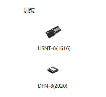
|
S-82K3/K4
Battery Protection IC for 3-serial or 4-serial Cell Pack with Constant Voltage Output Pin for Real-time Clock Enabling Any Order of Battery Connection (Secondary Protection) S-82K3/K4 Series Describes: This IC is used for secondary protection of lithium-ion rechargeable batteries, and incorporates high-accuracy voltage detection circuits and delay circuits. The S-82K3 Series enable connection of 3-serial cell, and the S-82K4 Series enable connection of 4-serial cell. This IC provides a wake-up function to prevent the fuse from blowing during battery connection, and allows the lithium battery to be connected in any order. Since this IC also comes with a constant voltage output circuit, it can be used as a constant-voltage power supply for an external RTC (Real-Time clock IC). Features: • High-accuracy voltage detection circuit for each cell Overcharge detection voltage n 3.600 V to 4.800 V (5 mV step) Accuracy ��15 mV (Ta = +25��C) Accuracy ��20 mV (Ta = −10��C to +60��C) Overcharge release voltage n*1 3.600 V to 4.800 V Accuracy ��50 mV VRTC pin shutdown voltage n 2.500 V to 2.800 V (100 mV step) Accuracy ��50 mV • The wake-up function monitoring battery connection prevents CO pin output errors during battery connection • Delay times for overcharge detection are generated only by an internal circuit (external capacitors are unnecessary) Overcharge detection delay time, VRTC pin shutdown delay time: 1s, 2s, 4s, 6s • Overcharge timer reset function: Available, unavailable • CO pin output voltage is limited to 7.5 V max. • VRTC pin output voltage: 1.800 V to 3.300 V (100 mV step) Accuracy ��2% (Ta = +25��C) • VRTC pin output current: 2 mA max. • Wide operation temperature range: Ta = −40��C to +85��C • Low current consumption During operation (VCU − 1.0 V for each cell): 4.0 ��A max. During VRTC pin shutdown (VRSD − 1.0 V for each cell): 1.0 ��A max. • Lead-free (Sn 100%), halogen-free *1. Overcharge release voltage = Overcharge detection voltage − Overcharge hysteresis voltage (Overcharge hysteresis voltage can be selected from a range of 0 mV to 400 mV in 50 mV step.) Remark n = 1, 2, 3, 4 Application: • Lithium-ion rechargeable battery packs (for secondary protection) |

|
S-82Y1A
Battery Protection IC for 1-Cell Pack S-82Y1B Series Describes: This IC is a protection IC for lithium-ion / lithium polymer rechargeable batteries, which includes high-accuracy voltage detection circuits and delay circuits. It is suitable for protecting 1-cell lithium-ion / lithium polymer rechargeable battery packs from overcharge, overdischarge, and overcurrent. Use of an external overcurrent detection resistor enables this IC to provide high-accuracy overcurrent protection with less impact from temperature changes. Features: • High-accuracy voltage detection circuit Overcharge detection voltage 3.500 V to 4.800 V (5 mV step) Accuracy ��15 mV Overcharge release voltage 3.100 V to 4.800 V*1 Accuracy ��50 mV Overdischarge detection voltage 2.000 V to 3.000 V (10 mV step) Accuracy ��50 mV Overdischarge release voltage 2.000 V to 3.400 V*2 Accuracy ��75 mV Discharge overcurrent 1 detection voltage 3 mV to 50 mV (0.25 mV step) Accuracy ��0.5 mV Discharge overcurrent 2 detection voltage 6 mV to 100 mV (0.5 mV step) Accuracy ��1.5 mV Load short-circuiting detection voltage 15 mV to 100 mV (1 mV step) Accuracy ��3.0 mV Charge overcurrent detection voltage −50 mV to −3 mV (0.25 mV step) Accuracy ��0.5 mV • Detection delay times are generated only by an internal circuit (external capacitors are unnecessary). • Discharge overcurrent control function Release condition of discharge overcurrent status: Load disconnection Release voltage of discharge overcurrent status: Discharge overcurrent release voltage (VRIOV) = VDD �� 0.8 (typ.) • 0 V battery charge: Enabled, inhibited • Power-down function: Available, unavailable • High-withstand voltage: VM pin and CO pin: Absolute maximum rating 28 V • Wide operation temperature range: Ta = −40��C to +85��C • Low current consumption During operation: 2.0 ��A typ., 4.0 ��A max. (Ta = +25��C) During power-down: 50 nA max. (Ta = +25��C) During overdischarge: 0.5 ��A max. (Ta = +25��C) • Lead-free (Sn 100%), halogen-free *1. Overcharge release voltage = Overcharge detection voltage − Overcharge hysteresis voltage (Overcharge hysteresis voltage can be selected as 0 V or from a range of 0.1 V to 0.4 V in 50 mV step.) *2. Overdischarge release voltage = Overdischarge detection voltage + Overdischarge hysteresis voltage (Overdischarge hysteresis voltage can be selected as 0 V or from a range of 0.1 V to 0.7 V in 100 mV step.) Applications: • Lithium-ion rechargeable battery pack • Lithium polymer rechargeable battery pack |
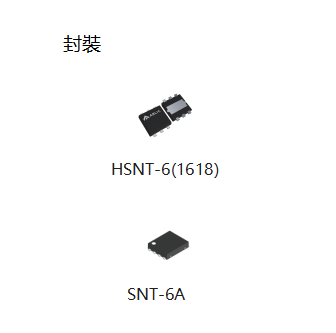
|
S-82K1B
Battery Protection IC for 1-Cell Pack S-82K1B Series Describes: The S-82K1B Series is a protection IC for lithium-ion / lithium polymer rechargeable batteries, which includes high-accuracy voltage detection circuits and delay circuits. It is suitable for protecting 1-cell lithium-ion / lithium polymer rechargeable battery packs from overcharge, overdischarge, and overcurrent. By using an external overcurrent detection resistor, the S-82K1B Series realizes high-accuracy overcurrent protection with less effect from temperature change. Features: • High-accuracy voltage detection circuit Overcharge detection voltage 3.500 V to 4.600 V (5 mV step) Accuracy ��15 mV Overcharge release voltage 3.100 V to 4.600 V*1 Accuracy ��50 mV Overdischarge detection voltage 2.000 V to 3.000 V (10 mV step) Accuracy ��50 mV Overdischarge release voltage 2.000 V to 3.400 V*2 Accuracy ��75 mV Discharge overcurrent detection voltage 1 0.003 V to 0.100 V (0.5 mV step) Accuracy ��1.0 mV Discharge overcurrent detection voltage 2 0.010 V to 0.100 V (1 mV step) Accuracy ��3 mV Load short-circuiting detection voltage 0.020 V to 0.100 V (1 mV step) Accuracy ��5 mV Charge overcurrent detection voltage −0.100 V to −0.003 V (0.5 mV step) Accuracy ��1.0 mV • Detection delay times are generated only by an internal circuit (external capacitors are unnecessary). • Discharge overcurrent control function Release condition of discharge overcurrent status: Load disconnection Release voltage of discharge overcurrent status: VRIOV = VDD �� 0.8 (typ.) • 0 V battery charge: Enabled, inhibited • Power-down function: Available, unavailable • High-withstand voltage: VM pin and CO pin: Absolute maximum rating 28 V • Wide operation temperature range: Ta = −40��C to +85��C • Low current consumption During operation: 2.0 ��A typ., 4.0 ��A max. (Ta = +25��C) During power-down: 50 nA max. (Ta = +25��C) During overdischarge: 0.5 ��A max. (Ta = +25��C) • Lead-free (Sn 100%), halogen-free *1. Overcharge release voltage = Overcharge detection voltage − Overcharge hysteresis voltage (Overcharge hysteresis voltage can be selected as 0 V or from a range of 0.1 V to 0.4 V in 50 mV step.) *2. Overdischarge release voltage = Overdischarge detection voltage + Overdischarge hysteresis voltage (Overdischarge hysteresis voltage can be selected as 0 V or from a range of 0.1 V to 0.7 V in 100 mV step.) Applications: • Lithium-ion rechargeable battery pack • Lithium polymer rechargeable battery pack |
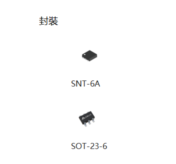
|
S-82C2A
Battery Protection IC for 2-serial-cell PacK S-82C2A Series Describes: This IC is a protection IC for lithium-ion / lithium polymer rechargeable batteries, which includes high-accuracy voltage detection circuits and delay circuits. It is suitable for protecting 2-serial-cell lithium-ion / lithium polymer rechargeable battery packs from overcharge, overdischarge, and overcurrent. Features: • High-accuracy voltage detection circuit Overcharge detection voltage n 3.500 V to 4.800 V (5 mV step) Accuracy ��20 mV Overcharge release voltage n 3.100 V to 4.800 V*1 Accuracy ��50 mV Overdischarge detection voltage n 2.000 V to 3.000 V (10 mV step) Accuracy ��50 mV Overdischarge release voltage n 2.000 V to 3.400 V*2 Accuracy ��75 mV Discharge overcurrent 1 detection voltage 3 mV to 400 mV (1 mV step) Accuracy ��3 mV Discharge overcurrent 2 detection voltage 10 mV to 400 mV (1 mV step) Accuracy ��5 mV Load short-circuiting detection voltage 20 mV to 800 mV (5 mV step) Accuracy ��10 mV Charge overcurrent detection voltage −400 mV to −3 mV (1 mV step) Accuracy ��3 mV • Detection delay times are generated only by an internal circuit (external capacitors are unnecessary). • 0 V battery charge: Enabled, inhibited • Power-down function: Available, unavailable • Release condition of discharge overcurrent status: Load disconnection, charger connection • Release voltage of discharge overcurrent status: Discharge overcurrent release voltage (VRIOV), discharge overcurrent 1 detection voltage (VDIOV1) • High-withstand voltage: VM pin and CO pin: Absolute maximum rating 28 V • Wide operation temperature range: Ta = −40��C to +85��C • Low current consumption During operation: 3.0 ��A typ., 6.0 ��A max. (Ta = +25��C) During power-down: 50 nA max. (Ta = +25��C) During overdischarge: 2.0 ��A max. (Ta = +25��C) • Lead-free (Sn 100%), halogen-free *1. Overcharge release voltage = Overcharge detection voltage − Overcharge hysteresis voltage (Overcharge hysteresis voltage can be selected as 0 V or from a range of 0.1 V to 0.4 V in 50 mV step.) *2. Overdischarge release voltage = Overdischarge detection voltage + Overdischarge hysteresis voltage (Overdischarge hysteresis voltage can be selected as 0 V or from a range of 0.1 V to 0.7 V in 100 mV step.) Remark n = 1, 2 Applications: • Lithium-ion rechargeable battery pack • Lithium polymer rechargeable battery pack |
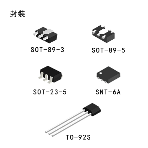
|
S-812C
High Operating Voltage CMOS Voltage Regulator S-812C Series Description The S-812C series is a family of high-voltage positive regulators developed using CMOS technology. The maximum operating voltage of 16V makes the S-812C series best in high-voltage applications. Not only current consumption is small but also power-off function is included, the regulator is also suitable in constructing low-power portable devices. Combination of power-off function and short-current protection can be selected. Features
Applications
|
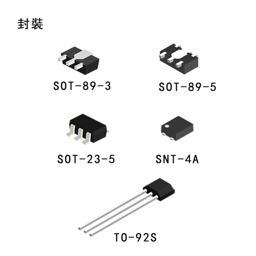
|
S-817
Ultra-Compact CMOS Voltage Regulator S-817 Series Description The S-817 Series is a 3-terminal positive voltage regulator, developed using CMOS technology. Small ceramic capacitors can be used as the output capacitor, and the S-817 series provides stable operation with low loads down to 1 ��A. Compared with the conventional voltage regulator, it is of low current consumption, and with a lineup of the super small package (SNT-4A:1.2 x 1.6mm). It is optimal as a power supply of small portable device. Features
Applications
|

|
S-816
External Transisor Type Voltage Regulator S-816 Series Description The S-816 series consists of external transistor type positive voltage regulators, which have been developed using the CMOS process. These voltage regulators incorporate an overcurrent protection, and power-off function. A low drop-out type regulator with an output current ranging from several hundreds of mA to 1A can be configured with the PNP transistor driven by this IC. Despite the features of the S-816, which is low current consumption, the improvement in its transient response characteristics of the IC with a newly deviced phase compensation circuit made it possible to employ the products of the S-816 series even in applications where heavy input variation or load variation is experienced. The S-816 series regulators serve as ideal power supply units for portable devices when coupled with the SOT-23-5 minipackage, providing numerous outstanding features, including low current consumption. Since this series can accommodate an input voltage of up to 16V, it is also suitable when operating via an AC adapter. Features
Applications
|

|
S-1112/1122
High Ripple-Rejection Low Dropout CMOS Voltage Regulator (LDO) S-1112/1122 Series Description The S-1112/1122 series is a positive voltage regulator with a low dropout voltage (LDO), high output voltage accuracy, and low current consumption developed based on CMOS technology. A built-in low on-resistance transistor provides a low dropout voltage and large output current, and a built-in overcurrent protector prevents the load current from exceeding the current capacitance of the output transistor. An ON/OFF circuit ensures a long battery life. Compared with the voltage regulators using the conventional CMOS process, a larger variety of capacitors are available, including small ceramic capacitors. Small SNT-6A(H) (S-1112 Series only), SOT-23-5 and 5-Pin SON(A) packages realize high-density mounting. In SOT-23-5 and 5-Pin SON(A), the lineup includes the S-1112 and S-1122 series, which differ in pin configuration. Features
Applications
|

|
S-1167
Ultra Low Current Consumption, High Ripple-Rejection Low Dropout (LDO) CMOS Voltage Regulator S-1167 Series Description The S-1167 Series is a positive voltage regulator with ultra low current consumption, high ripple rejection, low drop voltage (LDO) and high output voltage accuracy developed based on CMOS technology. Although current consumption is very small with 9 ��A typ., S-1167 Series realized the 70 dB of high ripple rejection rate. Besides a 1.0 ��F ceramic capacitor is available as an input-and-output capacitor. Moreover, dropout voltage is also small since output voltage accuracy realizes ��1.0% of high accuracy, and the low-on-resistance transistor is built-in. A built-in Output current protector prevents the load current from exceeding the current capacitance of the output transistor. A shutdown circuit ensures long battery life. Two packages, SOT-23-5 and SNT-6A(H), are available. Compared with the voltage regulators using the conventional CMOS process, S-1167 Series is the most suitable for the portable equipments with ultra low current consumption and corresponding to the small package. Features
Applications
|

|
S-11L10
Super-Low Output Low Dropout CMOS Voltage Regulator (LDO) S-11L10 Series Description S-11L10 Series, developed using the CMOS technology, is a positive voltage regulator IC which has the low output voltage (LDO), the high-accuracy output voltage and the low current consumption (150 mA output current). A 1.0 ��F small ceramic capacitor can be used. It operates with low current consumption of 9 ��A typ. The overcurrent protection circuit prevents the load current from exceeding the capacitance of output transistor. The power-off circuit ensures longer battery life. Various capacitors, also small ceramic capacitors, can be used for this IC more than for the conventional regulator ICs which have CMOS technology. Furthermore a small SOT-23-5 and SNT-6A(H) packages realize high-density mounting. Features
Applications
|
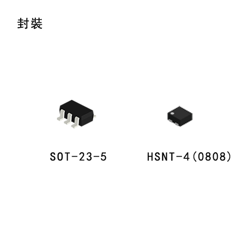
|
S-1312
Low Current Consumption High Ripple-Rejection Low Dropout CMOS Voltage Regulator S-1312 Series Description S-1312 Series, developed by using the CMOS technology, is a positive voltage regulator IC which has the low current consumption, the high ripple-rejection and the low dropout voltage. Even with low current consumption of 20 ��A typ., it has high ripple-rejection of 75 dB typ., and ceramic capacitor of 0.22 ��F or more can be used as the input and output capacitor. It also has high-accuracy output voltage of ��1.0%. Features
Applications
|
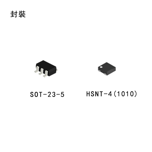
|
S-1312xxxH
105��C Operation Low Current Consumption High Ripple-Rejection Low Dropout CMOS Voltage Regulator S-1312xxxH Series Description The S-1312xxxH Series, developed by using the CMOS technology, is a positive voltage regulator IC which has low current consumption, high ripple-rejection and low dropout voltage. Features
Applications
|

|
S-1323
High Ripple-Rejection Small Package CMOS Voltage Regulator (LDO) S-1323 Series Description The S-1323 series is a positive voltage regulator with a low dropout voltage (LDO), high output voltage accuracy, and low current consumption developed based on CMOS technology. Features
Applications
|
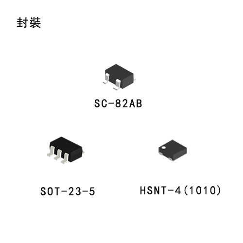
|
S-1335
High Ripple-Rejection Soft-Start Function CMOS Voltage Regulator S-1335 Series Description The S-1335 Series, developed by using the CMOS technology, is a positive voltage regulator IC of 150 mA output current, which has low dropout voltage, high-accuracy output voltage and soft-start function. The rising time of output voltage immediately after power-on or after the ON / OFF pin is set to ON is adjustable. A 1.0 ��F small ceramic capacitor can be used. It operates with low current consumption of 36 ��A typ. Furthermore the overcurrent protection circuit prevents the load current from exceeding the capacitance of output transistor. SOT-23-5, SC-82AB and super small HSNT-4 (1010) packages realize high-density mounting. Features
Applications
|

|
S-13R1
Reverse Current Protection CMOS Voltage Regulator S-13R1 Series Description The S-13R1 Series, developed by using the CMOS technology, is a positive voltage regulator IC of 150 mA output current, which has low dropout voltage, high-accuracy output voltage and low current consumption. Features
Applications
|

|
S-T111
High Ripple-Rejection and Low Dropout Voltage Regulator (LDO) S-T111 Series Description The S-T111 Series is a positive voltage regulator with a low dropout voltage (LDO), high output voltage accuracy, and low current consumption developed based on CMOS technology. Features
Applications
|
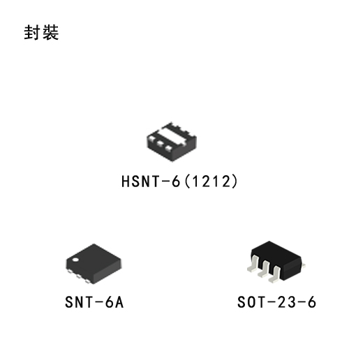
|
S-1200
High Ripple-Rejection and Low Dropout Low Input-and-Output Capacitance Voltage Regulator (LDO) S-1200 Series Description The S-1200 Series is a positive voltage regulator with a low dropout voltage (LDO), high output voltage accuracy developed based on CMOS technology. A 0.1 ��F small ceramic condenser can be used. It operates with low current consumption of 18 ��A typ. A built-in Output current protector prevents the load current from exceeding the current capacitance of the output transistor. Compared with the voltage regulators using the conventional CMOS process, small ceramic capacitors are also available. Furthermore a small HSNT-6A package realizes high-density mounting. Features
Applications
|

|
S-L2980
High Ripple-Rejection and Low Dropout Voltage Regulator (LDO) S-L2980 Series Description The S-L2980 series is a low dropout voltage regulator (LDO) designed for use in battery powered devices and developed using CMOS technology. On-chip low on-resistance transistor can provide low dropout voltage (LDO) and large output current. A power-off switch ensures long battery life. Features
Applications
|
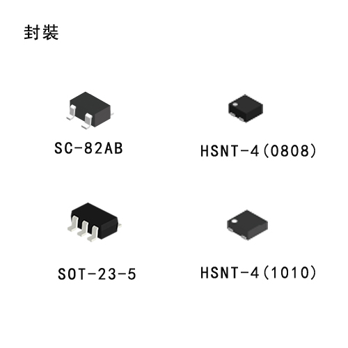
|
S-1313
Super Low Current Consumption Low Dropout CMOS Voltage Regulator S-1313 Series Description S-1313 Series, developed by using the CMOS technology, is a positive voltage regulator IC which has the super low current consumption and the low dropout voltage. Current consumption is as low as 0.9 ��A typ., and ceramic capacitor of 0.1 ��F or more can be used as the input and output capacitor. It also has high-accuracy output voltage of ��1.0%. Features
Applications
|
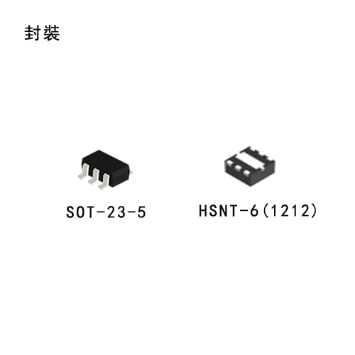
|
S-1315
Low Current Consumption Output Capacitor-Less CMOS Voltage Regulator S-1315 Series Description The S-1315 Series, developed by using the CMOS technology, is a positive voltage regulator IC of 200 mA output current which has low dropout voltage, high-accuracy output voltage and low current consumption. The S-1315 Series enables high density mounting due to output capacitor-less. The current consumption is extremely low as 7 ��A typ., and even without an output capacitor, it realizes high-speed response. It also has high-accuracy output voltage of ��1.0%. Features
Applications
|
|
S-1165
High Ripple-Rejection Low Dropout CMOS Voltage Regulator (LDO) S-1165 Series Description The S-1165 Series is a positive voltage regulator with a low dropout voltage (LDO), high output voltage accuracy, and low current consumption developed based on CMOS technology. A built-in low on-resistance transistor provides a low dropout voltage and large output current, and a built-in overcurrent protector prevents the load current from exceeding the current capacitance of the output transistor. An ON/OFF circuit ensures a long battery life, and a small SOT-23-5 package realizes high-density mounting. Features
Applications
|
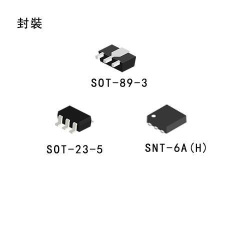
|
S-1206
Ultra Low Current Consumption and Low Dropout CMOS Voltage Regulator (LDO) S-1206 Series Description The S-1206 Series is a positive voltage regulator with ultra low current consumption, low dropout voltage (LDO), high output voltage accuracy, and 250 mA output current developed based on CMOS technology. I/O capacitors are as small as 0.1 ��F. S-1206 Series operates at ultra low current consumption of 1.0 ��s (typ.). The built-in low-on-resistance transistor realizes low dropout voltage and high output current. A built-in overcurrent protection circuit prevents the load current from exceeding the current capacitance of the output transistor. Three packages, SOT-23-3, SOT-89-3, and SNT-6A(H), are available. Compared with voltage regulators using a conventional CMOS process, more types of capacitors, including small I/O capacitors, can be used with the S-1206 Series. The S-1206 Series features ultra-low current consumption and comes in a small package, making them most suitable for portable equipment. Features
Applications
|
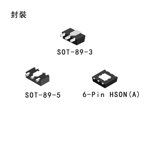
|
S-1131
High Ripple-Rejection Low Dropout Middle Output Current CMOS Voltage Regulator (LDO) S-1131 Series Description The S-1131 Series is a positive voltage regulator with a low dropout voltage (LDO), high output voltage accuracy, and low current consumption developed based on CMOS technology. Features
Applications
|
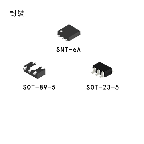
|
S-1132
High Ripple-Rejection Low Dropout Middle Output Current CMOS Voltage Regulator (LDO) S-1132 Series Description The S-1132 Series is a positive voltage regulator with a low dropout voltage (LDO), high output voltage accuracy, and low current consumption (300 mA output current) developed based on CMOS technology. A 0.1 ��F small ceramic capacitor can be used. It operates with low current consumption of 20 ��A typ. A built-in Output current protector prevents the load current from exceeding the current capacitance of the output transistor. Compared with the conventional 300 mA output current CMOS voltage regulators, high-density mounting is realized by using the super-small SNT-6A(H) package and a 0.1 ��F small ceramic capacitor. Also, the low current consumption makes the S-1132 series ideal for mobile devices. Features
Applications
|

|
S-1133
High Ripple-Rejection Low Dropout Middle Output Current CMOS Voltage Regulator (LDO) S-1133 Series Description The S-1133 Series is a positive voltage regulator with a low dropout voltage (LDO), high output voltage accuracy, and low current consumption (300 mA output current) developed based on CMOS technology. A 1 ��F small ceramic capacitor can be used. It operates with low current consumption of 60 ��A typ. The S-1133 Series includes an overcurrent protection circuit that prevents the output current from exceeding the current capacitance of the output transistor and a thermal shutdown circuit that prevents damage due to overheating. In addition to the types in which output voltage is set inside the IC, a type for which output voltage can be set via an external resistor is added to a lineup (S-1133��00 Series). SOT-89-5 and super-small SNT-8A package realizes a high density mounting. This, in addition to low current consumption, makes the S-1133 Series ideal for mobile devices. A ceramic capacitor of 2.2 ��F or more can be used for products whose output voltage is 1.7 V or less. Features
Applications
|
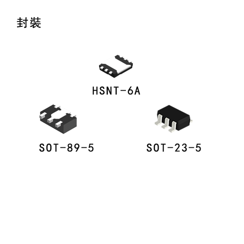
|
S-1135
High Ripple-Rejection Low Dropout Middle Output Current CMOS Voltage Regulator (LDO) S-1135 Series Description S-1135 Series, developed using the CMOS technology, is a positive voltage regulator IC which has the low dropout voltage (LDO), the high-accuracy output voltage and the low current consumption (300 mA output current). A 1.0 ��F small ceramic capacitor can be used. It operates with low current consumption of 45 ��A typ. The overcurrent protection circuit prevents the load current from exceeding the capacitance of output transistor. The power-off circuit ensures longer battery life. Various capacitors, also small ceramic capacitors, can be used for this IC more than for the conventional regulator ICs which have CMOS technology. Furthermore a small SOT-89-5, SOT-23-5, and HSNT-6A packages realize high-density mounting. Features
Applications
|

|
S-1137
High Ripple-Rejection Low Dropout Soft-start function CMOS Voltage Regulator (LDO) S-1137 Series Description S-1137 Series, developed using the CMOS technology, is a positive voltage regulator IC which has the low dropout voltage (LDO), the high-accuracy output voltage and the soft-start function (300 mA output current). A 1.0 ��F small ceramic capacitor can be used. It operates with low current consumption of 45 ��A typ. The overcurrent protection circuit prevents the load current from exceeding the capacitance of output transistor. The power-off circuit ensures longer battery life. Compared to the conventional CMOS technology regulator ICs, various capacitors including small ceramic capacitors can be used for this IC. Furthermore a small SOT-89-5, SOT-23-5, and SNT-6A(H) packages realize high-density mounting. Features
Applications
|
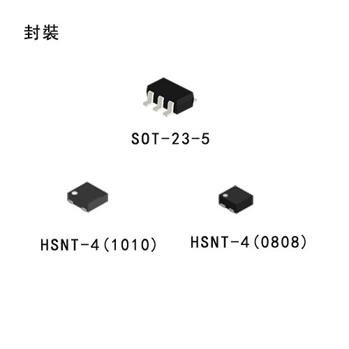
|
S-1333
Low Current Consumption High Ripple-Rejection Low Dropout CMOS Voltage Regulator S-1333 Series Description The S-1333 Series, developed by using the CMOS technology, is a positive voltage regulator IC which has low current consumption, high ripple-rejection and low dropout voltage. Even with low current consumption of 25 ��A typ., it has high ripple-rejection of 75 dB typ., and ceramic capacitor of 1.0 ��F or more can be used as the input and output capacitor. It also has high-accuracy output voltage of ��1.0%. Features
Applications
|

|
S-1155
High Ripple-Rejection Low Dropout High Output Current CMOS Voltage Regulator (LDO) S-1155 Series Description The S-1155 Series, developed based on CMOS technology, is a positive voltage regulator with a super low dropout voltage (LDO), high output voltageaccuracy, and low current consumption. The S-1155 Series provides the very small dropout voltage and the large output current due to the built-in transistor with low on-resistance. The overcurrent protector prevents the load current from exceeding the capacitance of output transistor. The thermal shutdown circuit prevents damage caused by heat, the rush current control circuit limits the excessive rush current during start-up. The ON/OFF circuit ensures longer battery life. Various capacitors, also small ceramic capacitors, can be used for this IC more than for the conventional regulator ICs which have CMOS technology. The small package SOT-89-5 enables high-density mounting. Features
Applications
|

|
S-1170
High Ripple-Rejection Low Dropout High Output Current CMOS Voltage Regulator (LDO) S-1170 Series Description The S-1170 Series is a positive voltage regulator with a low dropout voltage (LDO), high output voltage accuracy, and low current consumption developed based on CMOS technology. A built-in low on-resistance transistor provides a low dropout voltage and large output current, a built-in overcurrent protector prevents the load current from exceeding the current capacitance of the output transistor, and a built-in thermal shutdown circuit prevents damage caused by the heat. An ON/OFF circuit ensures a long battery life. Compared with the voltage regulators using the conventional CMOS process, a larger variety of capacitors are available, including small ceramic capacitors. Small SOT-89-5 and 6-Pin HSON(A) packages realize high-density mounting. Features
Applications
|
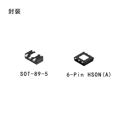
|
S-1172
High Ripple-Rejection Low Dropout High Output Current CMOS Voltage Regulator (LDO) S-1172 Series Description The S-1172 Series, developed based on CMOS technology, is a positive voltage regulator with a super low dropout voltage (LDO), high output voltage accuracy, and low current consumption. The S-1172 Series provides the very small dropout voltage and the large output current due to the built-in transistor with low on-resistance. The overcurrent protector prevents the load current from exceeding the capacitance of output transistor. The thermal shutdown circuit prevents damage caused by heat, the rush current control circuit limits the excessive rush current during start-up. The ON/OFF circuit ensures longer battery life. Compared with the voltage regulators using the conventional CMOS process, a large variety of capacitors are available, including small ceramic capacitors. High heat radiation HSOP-6 and small SOT-89-5 packages realize high-density mounting. Features
Applications
|
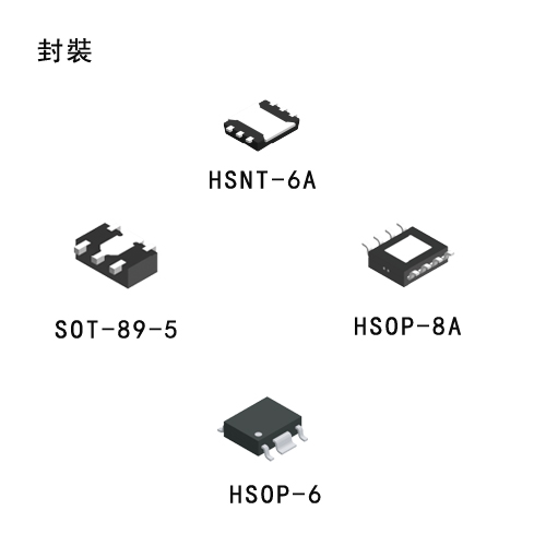
|
S-13A1
High Ripple-Rejection Low Dropout High Output Current CMOS Voltage Regulator S-13A1 Series Description The S-13A1 Series is a positive voltage regulator with a low dropout voltage, high output voltage accuracy, and low current consumption developed based on CMOS technology. A 2.2 ��F small ceramic capacitor can be used, and the very small dropout voltage and the large output current due to the built-in transistor with low on-resistance are provided. The S-13A1 Series includes a load current protection circuit that prevents the output current from exceeding the current capacitance of the output transistor and a thermal shutdown circuit that prevents damage due to overheating. In addition to the types in which output voltage is set inside the IC, a type for which output voltage can be set via an external resistor is added to a lineup. Also, the S-13A1 Series includes an inrush current limit circuit to limit the excess inrush current at power-on and at turn-on the ON/OFF pin. High heat radiation HSOP-8A, HSOP-6 and small SOT-89-5, HSNT-6A packages realize high-density mounting. Features
Applications
|

|
S-814
Low Dropout CMOS Voltage Regulator S-814 Series Description The S-814 series is a low dropout voltage, high output voltage accuracy and low current consumption positive voltage regulator (LDO regulator) developed utilizing CMOS technology. Features
Applications
|
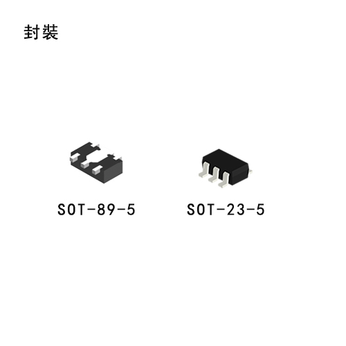
|
S-818
Low Dropout CMOS Voltage Regulator S-818 Series Description The S-818 series is a positive voltage regulator (LDO regulator) developed utilizing CMOS technology featured by low dropout voltage, high output voltage accuracy and low current consumption. Built-in low on-resistance transistor provides low dropout voltage and large output current. A ceramic capacitor of 2 ��F or more can be used as an output capacitor. A power-OFF circuit ensures long battery life. Features
Applications
|

|
S-1701
High Ripple-Rejection Low Dropout CMOS Voltage Regulator With Reset Function S-1701 Series Description The S-1701 Series, developed based on CMOS technology, is a voltage regulator with a reset function and integrates a high-accuracy voltage detector with on-chip delay circuit and a positive voltage regulator with a low dropout voltage and high output voltage on one chip. The S-1701 Series is available in many types according to the selection of the voltage detector block of the voltage detector, including a SENSE pin input product. A built-in low on-resistance transistor provides a low dropout voltage and large output current. Small ceramic capacitors are available and an external capacitor for delay is needless. Small SOT-23-5 and SOT-89-5 packages realize high-density mounting. Features Regulator block
Detector block
Whole regulator
Applications
|

|
S-1702
Ultra-Low Current Consumption 150 mA Voltage Regulator With Built-In High-Accuracy Voltage Detector and Reset Input Function S-1702 Series Description The S-1702 Series, developed based on CMOS technology, is a 150 mA output positive voltage regulator with a low dropout voltage, a high-accuracy output voltage, and low current consumption. Features
Detector block
Overall
Applications
|

|
S-1711
Super-Small Package 2-Circuit High Ripple-Rejection Low Dropout CMOS Voltage Regulator S-1711 Series Description The S-1711 Series is a 2-channel positive voltage regulator with a low dropout voltage, high output voltage accuracy, and low current consumption (150 mA output current) developed based on CMOS technology. A 1.0 ��F small ceramic capacitor can be used, and a 2-circuit voltage regulator with ��1.0% high-accuracy output voltage is incorporated in an SOT-23-6 or super-small SNT-6A package. The A/ B/ E/ F types are provided with a discharge shunt function allowing high-speed output response when the ON/OFF pin is used. Compared with the conventional 150 mA output current 2-channel CMOS voltage regulators, high-density mounting is realized by using the super-small SNT-6A package and a small ceramic capacitor. Also, the low current consumption makes the S-1711 Series ideal for mobile devices. Features
Applications
|

|
S-1721
Super-Small Package 2-Circuit High Ripple-Rejection Low Dropout CMOS Voltage Regulator S-1721 Series Description S-1721 Series, developed using the CMOS technology, is a 2-channel positive voltage regulator IC which has the low dropout voltage, the high-accuracy output voltage and the low output current consumption of 150mA. Users are able to use a small ceramic capacitor of 1.0 ��F for this IC. This IC includes two regulator circuits in the package SOT-23-6 or super-small SNT-6A. S-1721 Series has much lower current consumption than S-1711 Series, this IC is ideal for mobile devices. Features
Applications
|
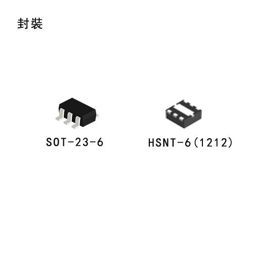
|
S-13D1
Super-Small Package 2-circuit Built-in Delay Function High Ripple-Rejection Low Dropout CMOS Voltage Regulator S-13D1 Series Description The S-13D1 Series, developed by using the CMOS technology, is a 2-channel positive voltage regulator IC which has low dropout voltage, high accuracy output voltage and low current consumption. Features
Applications
|
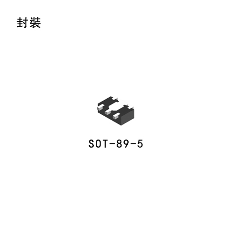
|
S-87X
High Withstand-Voltage Voltage Regulator with Reset Function S-87x Series Description The S-87x is a series of low-power high withstand-voltage regulators with a reset function, which integrates high-precision voltage detection and voltage regulation circuits on a single chip. The S-87x series has higher withstand-voltage characteristic and higher accuracy of detection voltage and output voltage, ��2.4% respectively. The S-87x series has also lineups for lithium-ion battery packs. Features
Applications
|
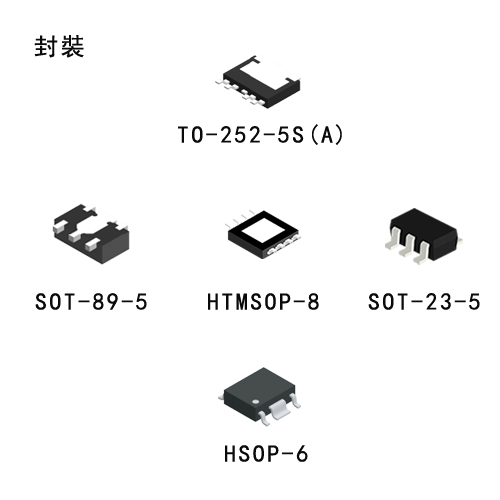
|
S-1212B/D
High-Withstand Voltage Low Current Consumption Low Dropout CMOS Voltage Regulator S-1212B/D Series Description The S-1212B/D Series, developed by using high-withstand voltage CMOS process technology, is a positive voltage regulator with a high-withstand voltage, low current consumption and high-accuracy output voltage, and has a built-in ON / OFF circuit. Features
Applications
|
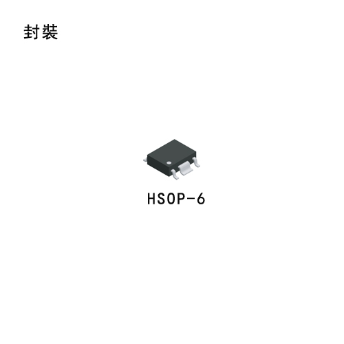
|
S-1142A/B
High-Withstand Voltage Low Current Consumption Low Dropout CMOS Voltage Regulator S-1142A/B Series Description S-1142A/B Series, developed based on high-withstand voltage CMOS process, is a positive voltage regulator with a high-withstand voltage, low current consumption, and high output voltage accuracy. S-1142A/B Series operates at a high maximum operating voltage of 50 V and a low current consumption of 4.0 ��A typ.. In addition to a built-in low on-resistance transistor which provides a very small dropout voltage and a large output current, this voltage regulator also has a built-in ON/OFF circuit. An overcurrent protector prevents the load current from exceeding the capacitance of the output transistor, and a built-in thermal shutdown circuit prevents damage caused by heat. A high heat radiation HSOP-6 package enables high-density mounting. Features
Applications
|

|
S-1142C/D
High-Withstand Voltage Low Current Consumption Low Dropout CMOS Voltage Regulator S-1142C/D Series Description S-1142C/D Series, developed based on high-withstand voltage CMOS process, is a positive voltage regulator with a high-withstand voltage, low current consumption, and high output voltage accuracy. S-1142C/D Series operates at a high maximum operating voltage of 50 V and a low current consumption of 4.0 ��A typ.. In addition to a built-in low on-resistance transistor which provides a very small dropout voltage and a large output current, this voltage regulator also has a built-in ON/OFF circuit. An overcurrent protector prevents the load current from exceeding the capacitance of the output transistor, and a built-in thermal shutdown circuit prevents damage caused by heat. A high heat radiation HSOP-6 package enables high-density mounting. Features
Applications
|
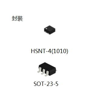
|
S-1318
5.5 V Input, 100 mA, 95 nA Super Low Current Consumption Voltage Regulator S-1318 Series Describe: The S-1318 Series, developed by using the CMOS technology, is a positive voltage regulator IC, which features super low current consumption and low dropout voltage. This IC has low current consumption of 95 nA typ. and high-accuracy output voltage of ��1.0%. It is most suitable for use in portable equipment and battery-powered devices. Features: • Output voltage: 1.2 V, 1.8 V, 2.2 V, 2.3 V, 2.5 V, 2.8 V, 3.0 V, 3.3 V • Input voltage: 1.7 V to 5.5 V • Output voltage accuracy: ��1.0% (1.2 V output product: ��15 mV) (Ta = +25��C) • Dropout voltage: 45 mV typ. (2.5 V output product, at IOUT = 10 mA) (Ta = +25��C) • Current consumption : During operation: 95 nA typ. During power-off: 2 nA typ. • Output current: Possible to output 75 mA (1.2 V output product, at VIN��VOUT(S + 1.0 V)*1 Possible to output 100 mA (1.8 V, 2.2 V, 2.3 V, 2.5 V, 2.8 V, 3.0 V, 3.3 V output product, at VIN��VOUT(S+ 1.0 V)*1 • Input capacitor: A ceramic capacitor can be used (1.0 ��F or more) • Output capacitor: A ceramic capacitor can be used (1.0 ��F or more) • Built-in overcurrent protection circuit: Limits overcurrent of output transistor • Built-in ON / OFF circuit: Ensures long battery life Discharge shunt function "available" / "unavailable" is selectable. Pull-down function "available" / "unavailable" is selectable. • Operation temperature range: Ta = −40��C to +85��C • Lead-free (Sn 100%), halogen-free *1. Please make sure that the loss of the IC will not exceed the power dissipation when the output current is large. Applications: • Constant-voltage power supply for battery-powered device • Constant-voltage power supply for portable communication device, digital camera, and digital audio player • Constant-voltage power supply for home electric appliance |
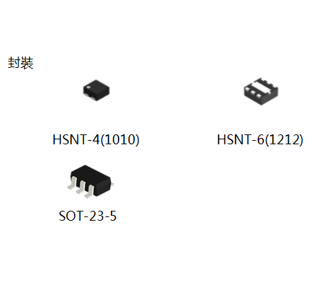
|
S-1740/S-1741
5.5 V Input, 100 mA Voltage Regulator with Supply Voltage Divided Output S-1740/1741 Series Describe: The S-1740/1741 Series, developed using CMOS technology, is a positive voltage regulator with the supply voltage divided output, which features super low current consumption and low dropout voltage. The regulator block has low current consumption of 0.35 ��A typ. and high-accuracy output voltage of ��1.0%. The function of the supply voltage divided output is prepared in the S-1740/1741 Series. The supply voltage divided output is a function that divides the input voltage (VIN) of the regulator into VIN/2 or VIN/3 and outputs the voltage. For example, this function makes it possible that the IC connects to a low voltage microcontroller A/D converter directly and the microcontroller monitors a battery voltage. Features: Regulator block • Output voltage: VOUT = 1.0 V to 3.5 V, selectable in 0.05 V step • Input voltage: VIN = 1.5 V to 5.5 V • Output voltage accuracy: ��1.0% (1.0 V to 1.45 V output product: ��15 mV) (Ta = +25��C) • Dropout voltage: 20 mV typ. (2.5 V output product, at IOUT = 10 mA) (Ta = +25��C) • Current consumption during operation: ISS1 = 0.35 ��A typ. (Ta = +25��C) • Output current: Possible to output 100 mA ( at VIN �� VOUT(S) + 1.0 V)*1 • Input capacitor: A ceramic capacitor can be used. (1.0 ��F or more) • Output capacitor: A ceramic capacitor can be used. (1.0 ��F to 100 ��F) • Built-in overcurrent protection circuit: Limits overcurrent of output transistor. Supply voltage divider block • Output voltage: VPMOUT = VIN/2 (S-1740 Series) VPMOUT = VIN/3 (S-1741 Series) • Current consumption during operation: ISS1P = 0.15 ��A typ. (Ta = +25��C) • Output capacitor: A ceramic capacitor can be used. (100 nF to 220 nF) • Built-in enable circuit: Ensures long battery life. Overall • Operation temperature range: Ta = −40��C to +85��C • Lead-free (Sn 100%), halogen-free *1. Please make sure that the loss of the IC will not exceed the power dissipation when the output current is large. Applications: • Constant-voltage power supply and battery voltage monitoring support for battery-powered device • Constant-voltage power supply for portable communication device, digital camera, and digital audio player • Constant-voltage power supply for home electric applianc |
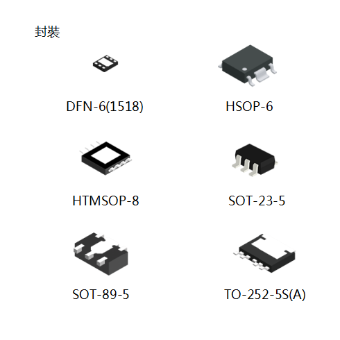
|
S-1222B/D
28 V Input, 200 mA Voltage Regulator S-1222B/D Series Describe: The S-1222B/D Series, developed by using high-withstand voltage CMOS process technology, is a positive voltage regulator with a high-withstand voltage, low current consumption and high-accuracy output voltage, and has a built-in ON / OFF circuit. The S-1222B/D Series operates at the maximum operation voltage of 28 V and a low current consumption of 6.5 ��A typ., and has a built-in low on-resistance output transistor which provides a very small dropout voltage and a large output current. Also, a built-in overcurrent protection circuit to limit overcurrent of the output transistor and a built-in thermal shutdown circuit to limit heat are included. Features: • Output voltage: 2.3 V to 12.0 V, selectable in 0.1 V step • Input voltage: 3.0 V to 28 V • Output voltage accuracy: ��1.0% (Ta = +25��C) • Current consumption: During operation: 6.5 ��A typ. (Ta = +25��C) During power-off: 0.1 ��A typ. (Ta = +25��C) • Output current: Possible to output 200 mA (at VIN �� VOUT(S) + 2.0 V)*1 • Input capacitor: A ceramic capacitor can be used. (1.0 ��F or more) • Output capacitor: A ceramic capacitor can be used. (1.0 ��F to 100 ��F) • Built-in overcurrent protection circuit: Limits overcurrent of output transistor. • Built-in thermal shutdown circuit: Detection temperature 165��C typ. • Built-in ON / OFF circuit: Ensures long battery life. Discharge shunt function is available. • Operation temperature range: Ta = −40��C to +85��C • Lead-free, Sn 100%, halogen-free *1. Please make sure that the loss of the IC will not exceed the power dissipation when the output current is large. Applications: • Constant-voltage power supply for industrial equipment • Constant-voltage power supply for home electric appliance • Constant-voltage power supply for smartcard |
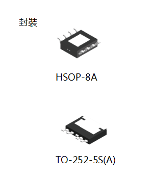
|
S-1214
105��C Operation, 36 V Input, 1000 mA Voltage Regulator S-1214 Series Describe: The S-1214 Series developed by using high-withstand voltage CMOS process technology, is a positive voltage regulator with a high-withstand voltage, low current consumption and high-accuracy output voltage. The S-1214 Series operates at the maximum operation voltage of 36 V and a low current consumption of 5.0 ��A typ. and has a built-in low on-resistance output transistor, which provides a very small dropout voltage and a large output current. In addition to the type in which output voltage is set inside the IC, the type for which output voltage can be set via an external resistor is added to a lineup. Also, a built-in overcurrent protection circuit to limit overcurrent of the output transistor and a built-in thermal shutdown circuit to limit heat are included. Features: • Output voltage (internally set): 1.8 V, 3.0 V, 3.3 V, 5.0 V, 8.0 V, 12.0 V, 15.0 V • Output voltage (externally set): 1.8 V to 30.0 V, settable via external resistor • Input voltage: 2.8 V to 36.0 V • Output voltage accuracy: ��1.0% (Ta = +25��C) • Current consumption: During operation: 5.0 ��A typ.(Ta = +25��C) During power-off: 0.1 ��A typ.(Ta = +25��C) • Output current: Possible to output 1000 mA (at VIN �� VOUT(S) + 2.0 V)*1 • Input and output capacitors: A ceramic capacitor can be used. (1.0 ��F or more) • Built-in overcurrent protection circuit: Limits overcurrent of output transistor. (with a detection function of the difference between input and output voltage) • Built-in thermal shutdown circuit: Detection temperature 170��C typ. • Built-in ON / OFF circuit: Ensures long battery life. Discharge shunt function is available. Pull-down function is available. • Operation temperature range: Ta = −40��C to +105��C • Lead-free (Sn 100%), halogen-free *1. Please make sure that the loss of the IC will not exceed the power dissipation when the output current is large. *2. Contact our sales representatives for details. Applications: • Constant-voltage power supply for industrial equipment • Constant-voltage power supply for home electric appliance |